

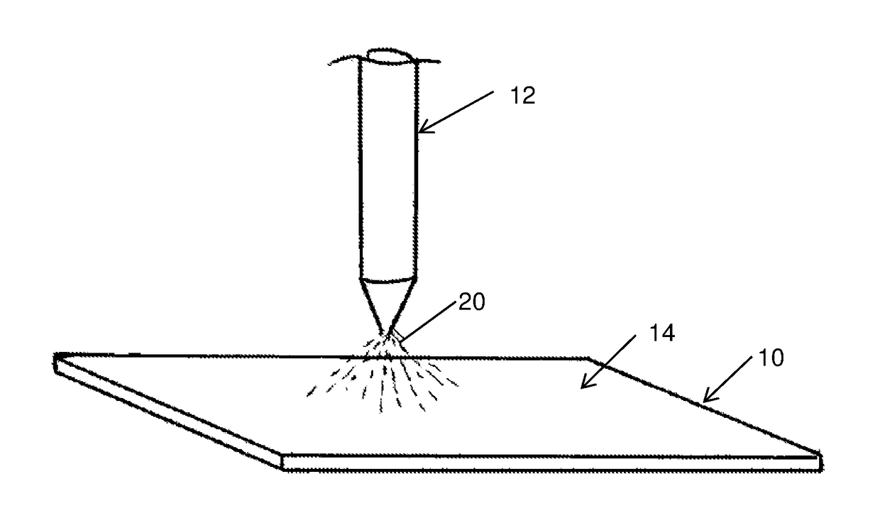
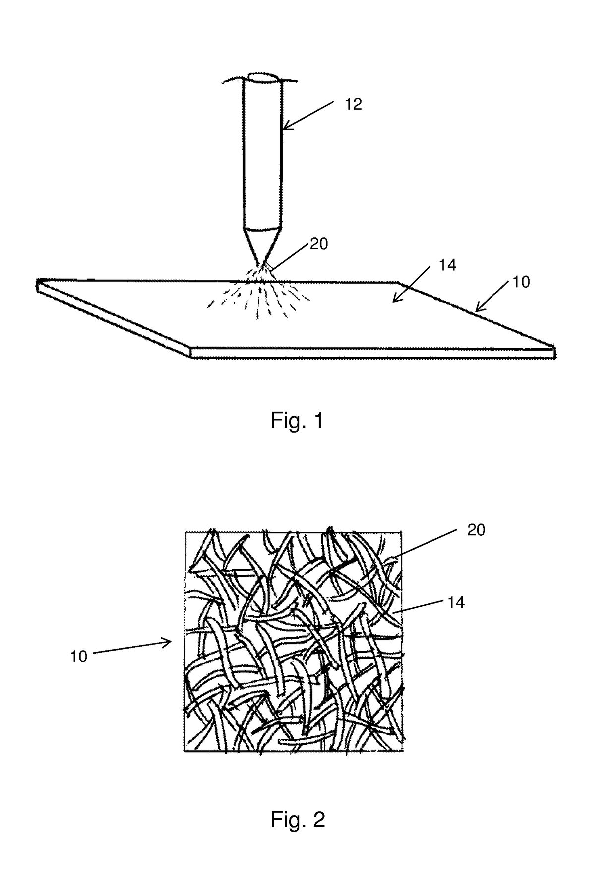
Low reflectivity coating and method and system for coating a substrate
a technology of low reflectivity and substrate, applied in the direction of coatings, optical elements, instruments, etc., can solve the problems of limiting commercial applications, faulty or lowering the performance of catalysts beyond an acceptable threshold, and requiring even more complex catalyst steps
- Summary
- Abstract
- Description
- Claims
- Application Information
AI Technical Summary
Benefits of technology
Problems solved by technology
Method used
Image

Examples
example 2
mple
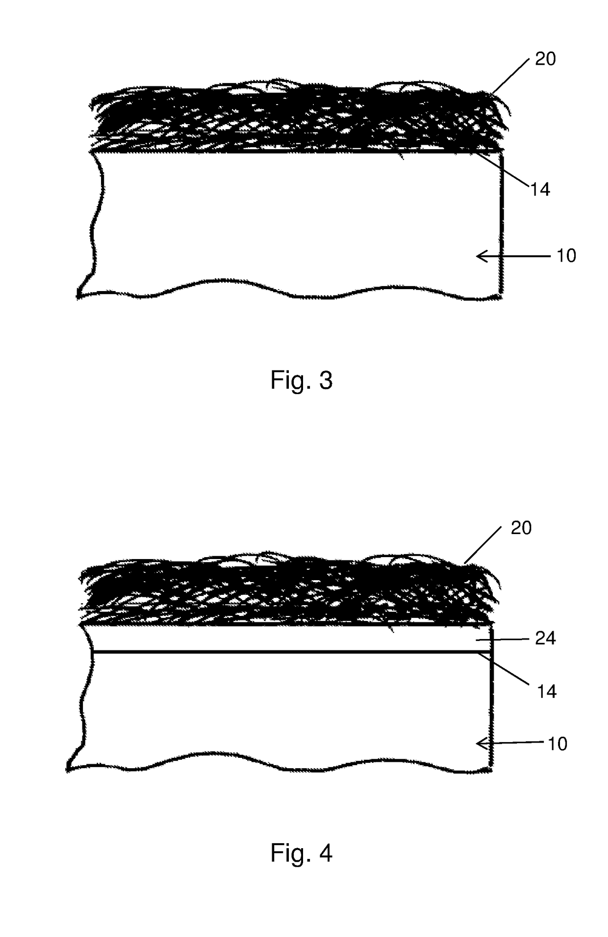
[0115]An aluminium 6061 grade coupon was sprayed according to the procedure set out in Comparative Example 1 until the mass of the coating on the substrate was 1.13 mgcm−2. The coating was then subject to an oxygen etch in a plasma reaction chamber (NanoGrowth 400 Etch) to generate the required optical cavities. The etching process comprised a 7 minute oxygen etch at a pressure of 0.3 Torr and a power density of 0.12 Wcm−2. Following this the resultant sample was hydrophobically coated, in the same plasma chamber, for 5 minutes in a carbon tetrafluoride plasma at a pressure of 0.3 Torr and 250° C. substrate temperature with a power density of 0.12 Wcm−2.
[0116]The THR of the resulting coating was measured as for Comparative Example 1 above and the results are shown in FIGS. 18 and 19. It can be seen that the THR is significantly reduced compared to Example 1.
example 3
ed Sample
[0117]An aluminium 6061 grade coupon as above was sprayed according to the procedure set out in Comparative Example 1 until the mass of the coating on the substrate was 0.33 mgcm−2. The sample was then oxygen etched and hydrophobically coated as for Example 2.
[0118]The THR of the resulting coating was measured as for Comparative Example 1 above and the results are shown in FIGS. 18 and 19.
[0119]The result is a significant over-etch and as a result the reflectance values are increased (but are still lower than those of Example 1).
example 4
hed Sample
[0120]An aluminium 6061 grade coupon was sprayed according to the procedure set out in Comparative Example 1 until the mass of the coating on the substrate was 1.07 mgcm−2. The coating was then etched in an oxygen plasma as before for 7 minutes at a pressure of 0.3 Torr but a reduced power density of 0.045 Wcm−2.
[0121]The sample was then oxygen etched and hydrophobically coated as for Example 2.
[0122]The THR of the resulting coating was measured as for Comparative Example 1 above and the results are shown in FIGS. 18 and 19.
[0123]The result is that fewer optical cavities are created and thus the reflectance values do not reach optimum levels (but are still lower than those of Example 1).
PUM
| Property | Measurement | Unit |
|---|---|---|
| thickness | aaaaa | aaaaa |
| temperature | aaaaa | aaaaa |
| concentration | aaaaa | aaaaa |
Abstract
Description
Claims
Application Information