
High performance computing network

a computing network and high-performance technology, applied in computing, digital computers, instruments, etc., can solve the problems of system processing speed limitation, important software overhead and limitations, schism amongst users, etc., to achieve the highest possible speed, reduce processing delays, and improve processing speed

Active Publication Date: 2019-05-09
NANOTRONIX INC
View PDF1 Cites 0 Cited by
  • Summary
  • Abstract
  • Description
  • Claims
  • Application Information

AI Technical Summary

Benefits of technology

The present invention is a computer system that uses a combination of Ethernet interconnects and parallel processing nodes to achieve higher processing speed. The system can be easily scaled up by adding more nodes, and the processing speed is limited by the speed at which data can be transferred between nodes. The system also provides a highly deterministic operational framework for processing and data acquisition applications. The technical effects of the invention include higher processing speed, scalability, and efficient allocation of hardware resources.

Problems solved by technology

This kind of centralisation has made CPU task-sharing (or multitasking) a necessity, introducing management complexities in modern operating systems and programming models, further causing important software overheads and limitations in per-task execution granularity and task-completion determinism to be considered as acceptable trade-offs.
These later characteristics have also generated a schism among computing hardware designed for general use and hardware designed for data acquisition, control automation or other applications in need for real-time and predictable handling of computing loads.
These CPU-centric computer architectures are heavily focussed on CPUs directing all processes within the computer and, as such, the system's processing speed is limited, in part, by the speed of the CPU.
This hardware has taken the form of graphics processors, expansion-bus interfaces and memory controllers integrated in modern CPUs, making them highly complicated Systems-on-Chip (SoC), while always remaining aligned to the general architectural principle of a CPU-centric motherboard system.
Even though this kind of integration has made low-power and mobile computing possible, it hasn't provided a realistic path forward for data centre and industrial scale computing which, contrary to mobile computing and, in part, in order to complement it by (cloud) abstraction, has had to grow and adapt to handling extremely diverse, complex and always evolving sets of computing loads in the most power efficient way.
However, due to the CPU / Motherboard-centric model of current computer architecture, FPGAs / ASICs remain on the periphery of computing hardware, limited mostly to offering acceleration and off-loading services to the CPU.
However, these interconnects impose physical limitations to scaling (as interconnection points are limited by the size of the motherboard), and lack the mechanisms for supporting peer importance component interaction (such as uniform access to memory), introducing further constrains in resource accessibility and combined resource utilisation.
Ideally, but not always, this process will run with the CPU handing over memory control to the further processing element for accessing the memory directly (via direct memory access (DMA)), even though memory controller integration in modern (SoC) CPUs is blurring this line, and the extensive use of caching further raises various challenges on data coherence, synchronisation and avoiding performance penalties over such a transaction.
Attaching FPGAs / ASICs as peripheral equipment to CPU-centric computing systems hinders their performance and limits their importance in modern computing.
FPGAs / ASICs are designed, at component and even internal circuitry level, to operate extremely efficiently in parallel while scale in numbers, but attachment points available to CPU-based systems, typically through expansion boards over PCIe slots, are very limited.
This forces extensive hardware multiplexing, which does not permit efficient parallelization or scaling, to be used in order to orchestrate operation:many FPGA / ASIC carrying expansion boards are multiplexed over the limited PCIe lanes available to the CPU (CPU motherboard level multiplexing);many FPGA / ASICs, at expansion board level, are multiplexed over the PCIe lanes assigned to each expansion board.
Such systems are complex to build and program, as well as power inefficient to run.

Method used


Image

  • High performance computing network
  • High performance computing network
  • High performance computing network

Examples


Embodiment Construction

[0030]As the processing capabilities and power efficiency of FPGAs and ASICs increase, their use in computer systems is becoming more common. In this manner, an FPGA / ASIC based acceleration board is connected to a CPU-centric motherboard, usually within a client or server computer, for offloading computationally intensive parts of an application from the CPU, or for real-time processing of data intended for data acquisition and machine automation. FPGAs / ASICs are connected to the CPU through high-speed backplanes or board-to-board interconnects, e.g. PCI Express (PCIe), as expansion boards. This kind of interfacing introduces hard architectural constraints on scalability.

[0031]Connection through a PCIe bus is an attractive choice for tightly coupled accelerators due to its high throughput capacity. However PCIe is a complicated and expensive interconnect technology. Furthermore because there is no standard host-FPGA communication library, FPGA developers have to write significant am...


PUM


Abstract

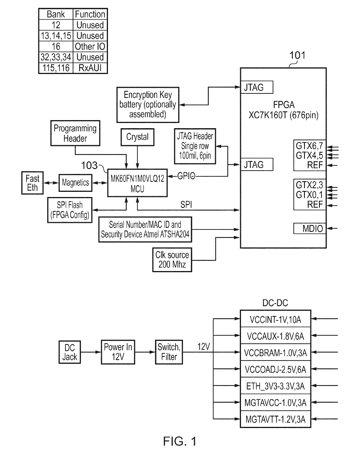
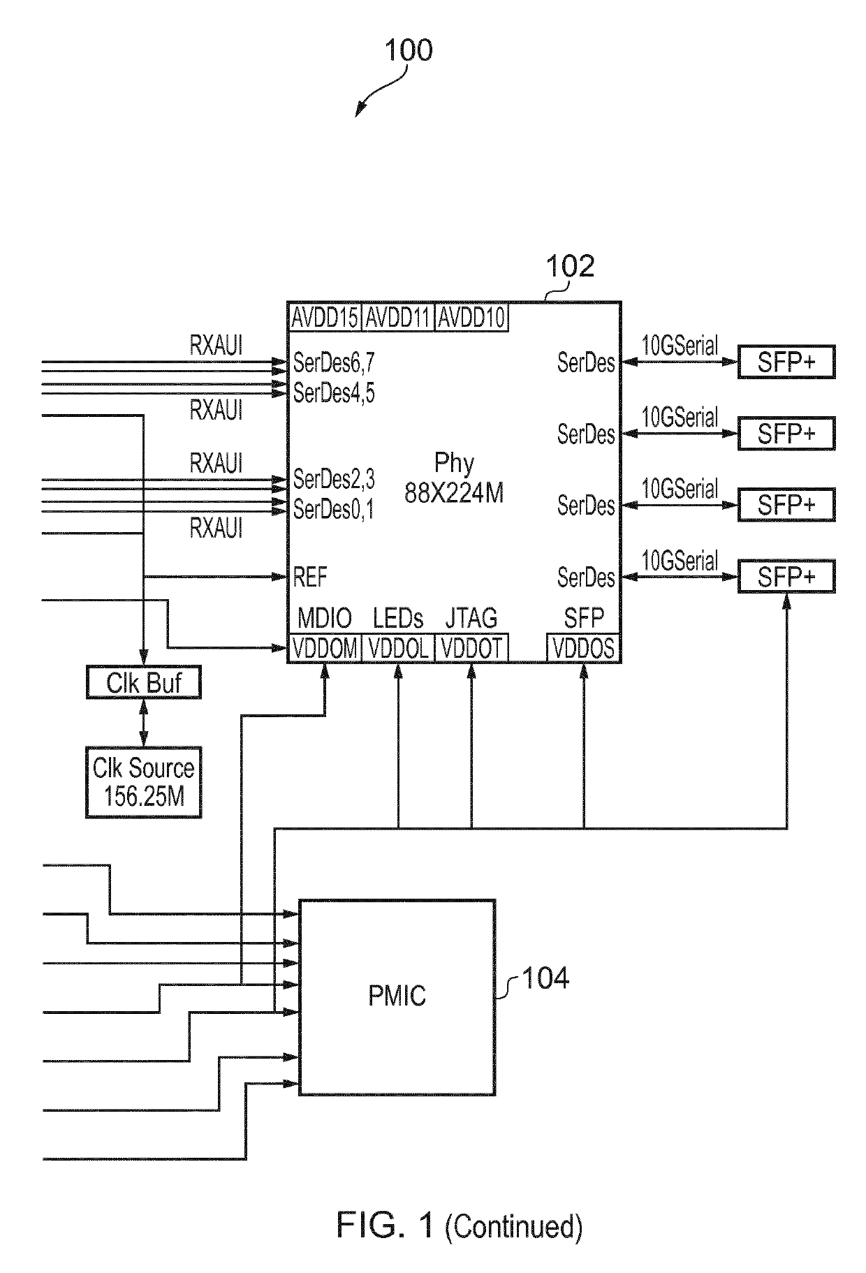
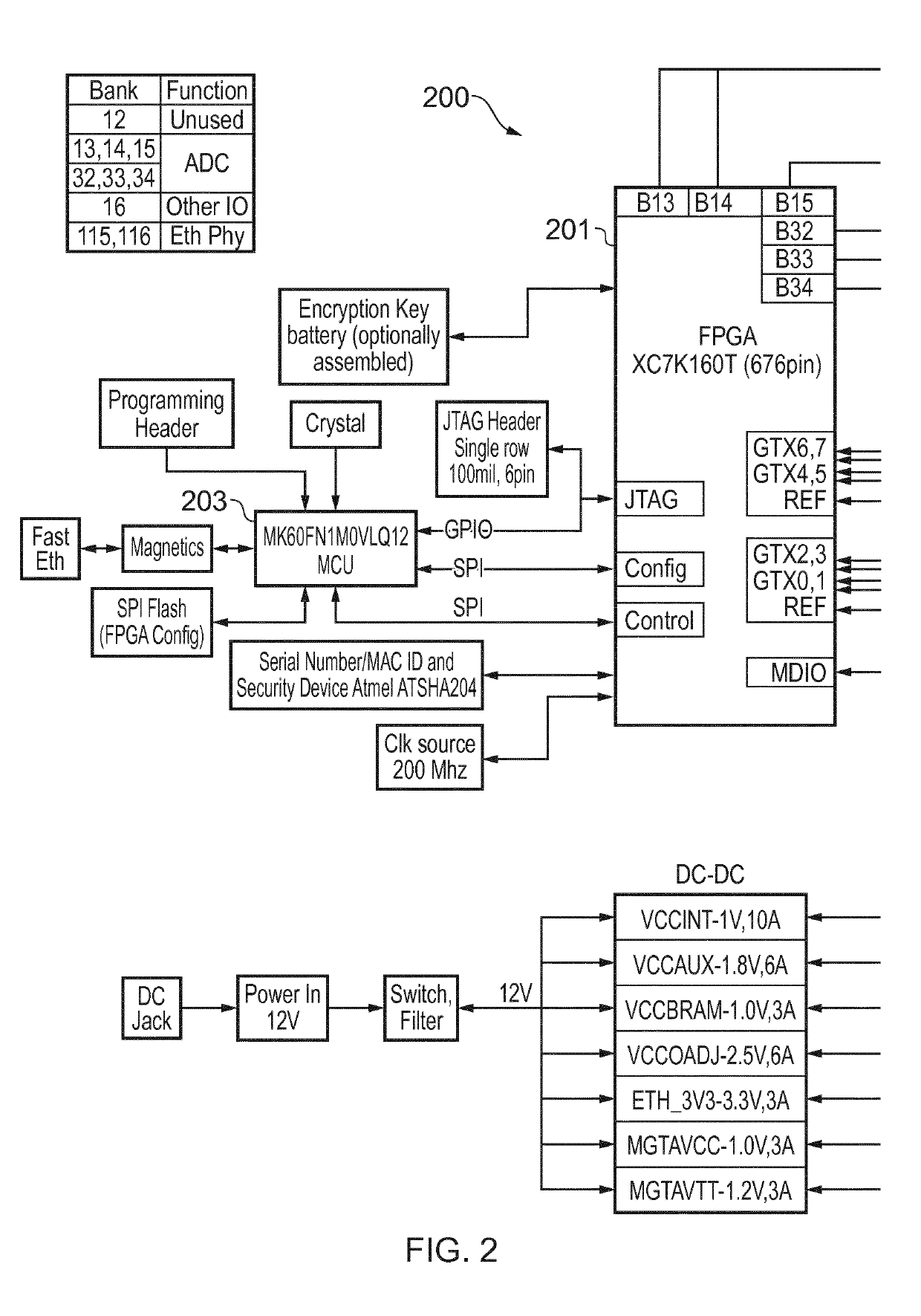
The present invention relates to a method of processing data in a computer system, the method comprising the steps of: 1) allocating at least one processing node (100); 2) receiving data at a data source node (200, 400); 3) transferring the data to the or each processing node (100) through a serial data connection; 4) processing the data at the or each processing node (100); and 5) transferring the processed data from the or each processing node (100) to a data sink node (300, 400) through the serial data connection, wherein the at least one processing node (100), the data source node (200, 400) and the data sink (300, 400) each comprise no more than one Field Programmable Gate Array (101) or Application Specific Integrated Circuit.

Description

FIELD OF THE INVENTION[0001]The present invention relates generally to a new computer architecture. More specifically, the invention relates to a nodal FPGA / ASIC based computer architecture.BACKGROUND OF THE INVENTION[0002]Conventional computing systems are based on Von Neumann or Harvard architectures. Both of these systems rely on a Central Processing Unit (CPU) to direct any processes occurring within the system. For the better part of the last four decades, computing, scaling from personal to data-center sized systems, has evolved around a CPU-centric motherboard, with everything else intended for data processing or storage, operating in the periphery of the CPU. This kind of centralisation has made CPU task-sharing (or multitasking) a necessity, introducing management complexities in modern operating systems and programming models, further causing important software overheads and limitations in per-task execution granularity and task-completion determinism to be considered as a...

Claims


Application Information

Patent Timeline
Patent Type & Authority Applications(United States)
IPC IPC(8): G06F13/20G06F13/42
CPCG06F13/20G06F13/4282G06F15/17375G06F15/82
Inventor ANGELAKOS, EVANGELOSMASSELOS, KONSTANTINOS
Owner NANOTRONIX INC
Learn More