

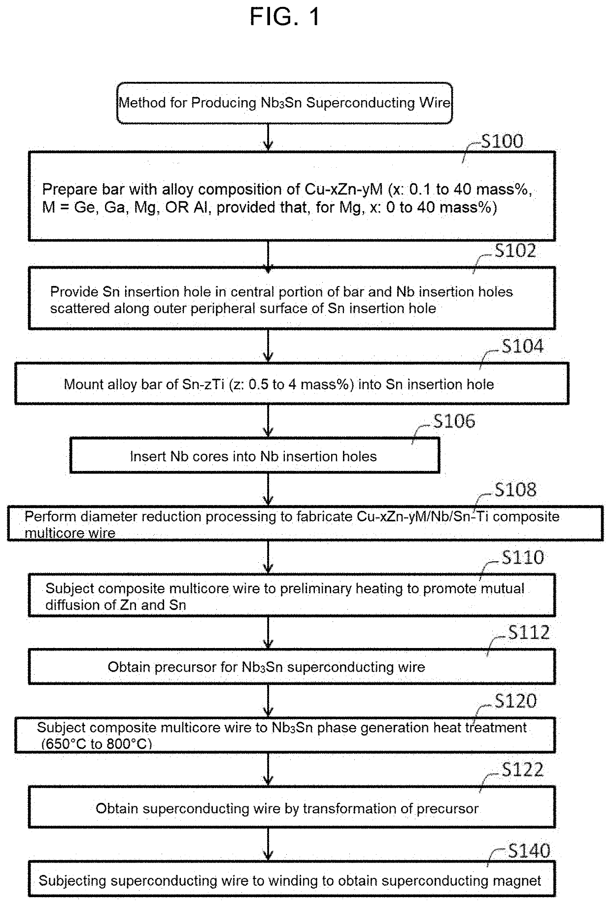
METHOD FOR PRODUCING Nb3Sn SUPERCONDUCTING WIRE, PRECURSOR FOR Nb3Sn SUPERCONDUCTING WIRE, AND Nb3Sn SUPERCONDUCTING WIRE USING SAME
a superconducting wire and superconducting wire technology, applied in the direction of superconductors/hyperconductors, superconductors, transportation and packaging, etc., can solve the problems of difficult to increase the volume of nb/sub>3/sub>sn, difficult to produce a wire, and brittleness of 3/sub>sn as a superconducting wire, etc., to achieve improved critical temperature, increase interface resistance, and high functional
- Summary
- Abstract
- Description
- Claims
- Application Information
AI Technical Summary
Benefits of technology
Problems solved by technology
Method used
Image

Examples
example 1
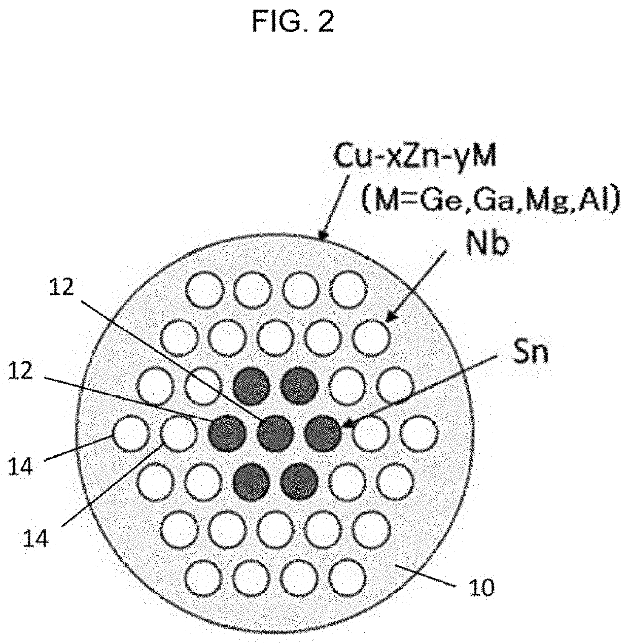
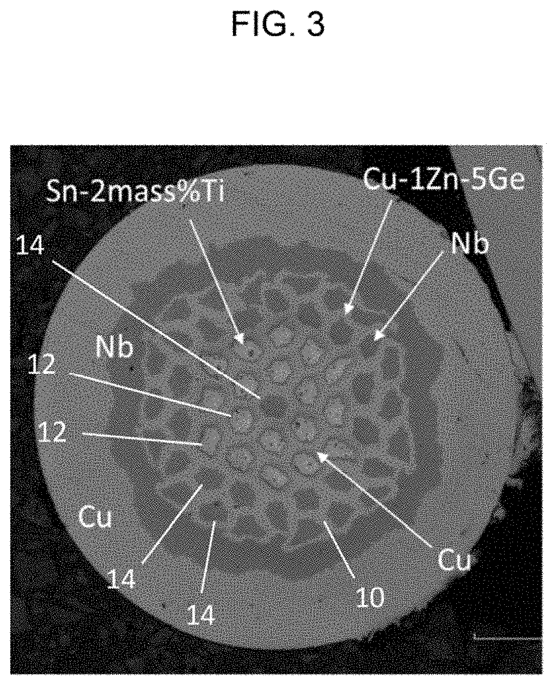
[0066]A precursor having the cross-sectional configuration shown in FIG. 3 was fabricated in accordance with the procedure mentioned below. First, a bar made of Cu-1Zn-5Ge with an outer diameter of 30 mm (provided that, in the present Example, copper was placed in a central portion in order to improve processability) was prepared as the matrix 10 (S100). Next, a hole with an inner diameter of 2 mm was formed in a central portion of the matrix 10 to form a Nb insertion hole. Next, a total of twenty holes were formed along a first outer periphery and a second outer periphery around the central hole, and Sn insertion holes 12 were formed. Further, a total of 36 Nb insertion holes 14 were provided between a third outer periphery located on the outer periphery of the Sn insertion holes 12 and a fourth outer periphery on the inside of the outer peripheral surface of the bar made of Cu-1Zn-5Ge, which was the matrix (S102). That is, there were 37 Nb insertion holes 14 in total.
[0067]Next, a...
example 2
[0073]A composite precursor wire with a wire diameter of 0.814 mm similarly produced using a Cu-1Zn-10Ga alloy matrix was subjected to preliminary heating of 650° C.×100 h in an Ar gas atmosphere, and was then subjected to heat treatment of 750° C.×100 h in order to produce a Nb3Sn layer.
[0074]The result of composition mapping has shown that, in the case of Ga, Ga diffuses to the Nb3Sn layer after the heat treatment. A magnetization-temperature curve of the present sample was measured by SQUID, and it has been found that, as shown in FIG. 5, the critical temperature at which a superconducting state is created was increased by 0.3 K as compared to the case where Ga was not added.
example 3
[0075]A composite precursor wire similarly produced using a Cu-0.2Zn-1Mg alloy matrix was subjected to preliminary heating of 650° C.×100 h in an Ar gas atmosphere, and was then subjected to heat treatment of 800° C.×20 h in order to produce a Nb3Sn layer.
[0076]SEM observation was performed on a fracture surface of the wire, and it has been found that the average grain diameter of a Cu matrix in which Mg was not added was approximately 500 nm or more. On the other hand, in the matrix in which Mg was added, the grain coarsening was suppressed, and the average grain diameter was approximately 300 nm.
PUM
| Property | Measurement | Unit |
|---|---|---|
| Temperature | aaaaa | aaaaa |
| Percent by mass | aaaaa | aaaaa |
| Percent by mass | aaaaa | aaaaa |
Abstract
Description
Claims
Application Information