Semiconductor fab's defect operating system and method thereof

Active Publication Date: 2020-01-23
ELITETECH TECH
View PDF0 Cites 6 Cited by
  • Summary
  • Abstract
  • Description
  • Claims
  • Application Information

AI Technical Summary

Benefits of technology

The invention provides a business model for improving defect screening in semiconductor manufacturing. The model allows IC design houses to join a wafer shuttle program and work with semiconductor fabrics to solve systematic defect problems. This results in early pilot production, market share gain, and revenue increase. The model also allows IC design houses to monitor all process layers' random defects and defect type information, which is important for improving wafer yield. The cooperation between semiconductor fab and IC design houses can quickly improve wafer yield.

Problems solved by technology

Obviously, IC design house authorize semiconductor Fab to manufacture wafer, but IC design house doesn't invest to build Fab or purchase equipment tools.
In the manufacturing procedure, random defect and systematic defect are produced probably because of resolution deviation of equipment itself, abnormal incidence, particle induced in a process, pattern defect in the design layout pattern, and insufficient lithography process window.
Those defects will cause open or short failure die.
If the engineering department resource and experience are insufficient, semiconductor Fab cannot achieve the expected wafer yield target.
Then, it could delay the pilot production or the schedule to be on the market.
Based on current manufacturing procedure, the semiconductor Fab and IC design house might not be able to increase revenue and profit earlier when the capability to resolve defect issue in a semiconductor Fab is insufficient.
But, Fab did not release this potential wafer risk information or various metrology information o customers (IC design houses).
But, those information impacting wafer yield, like defect data, line width, thickness data are not provided to IC design houses.
For example: Abnormal equipment problem leads to low wafer yield problem.
However, this low wafer yield problem impacts on-time delivery to design house's customer after the incidence happened a few weeks ago.
Currently, the management of semiconductor Fab by an IC design house is only limited to trace wafer progress.
In term of on-time wafer delivery, design house lacks a real-time monitor apparatus to monitor defect data and abnormal wafer lot.
But, there is no method or system available.
It becomes worse especially when semiconductor technology migrates to nanometer scale.
The immersion scanner, multi-exposure techniques, and process, optical proximity correction, layout pattern interaction makes the systematic defect and random defect failure much more complex.
Obviously, if the management of semiconductor Fab by IC design house is still the same as before (semiconductor Fab in charge of all the defect issue) and not involved on the defect problem solution, then the time to improve wafer yield cannot be shortened.
It will delay the delivery time of product from an advanced process Fab.
Following the shrinked geometry size toward advanced semiconductor process, systematic defect issue becomes a more and more severe problem.
In addition, the characteristic of systematic defect is that the systematic defects will happen at various repeated defect pattern locations.
So, there are many systematic defect patterns happen at various design layout pattern groups.
Because of the slow imaging throughput of Scanning Electron Microscope (SEM), SEM throughput limitation leads to defect sample selection in a semiconductor Fab.
Obviously, it is very difficult to find the real open or short failure systematic defect through such defect sample selection procedure.
If the real systematic defect is not inside the 500 defect design layout pattern groups, then semiconductor Fab cannot immediately provide accurate systematic defect SEM images to process engineer.
Based on those SEM images, there is no way Fab can judge root cause of systematic defect, either from process, optical proximity correction, or layout pattern problem.
This will delay the time to improve systematic defect yield problem.
In the end, this raises cost of semiconductor Fab and IC design house.
Similarly, the slow SEM imaging throughput of SEM limits the defect sample selection quantities, i.e. only several tens to several hundred defect samples will be selected for SEM imaging.
But, that method can hardly find failure killer random defect in the defect analysis of nanometer scale semiconductor process.

Method used


Image

  • Semiconductor fab's defect operating system and method thereof
  • Semiconductor fab's defect operating system and method thereof
  • Semiconductor fab's defect operating system and method thereof

Examples


Embodiment Construction

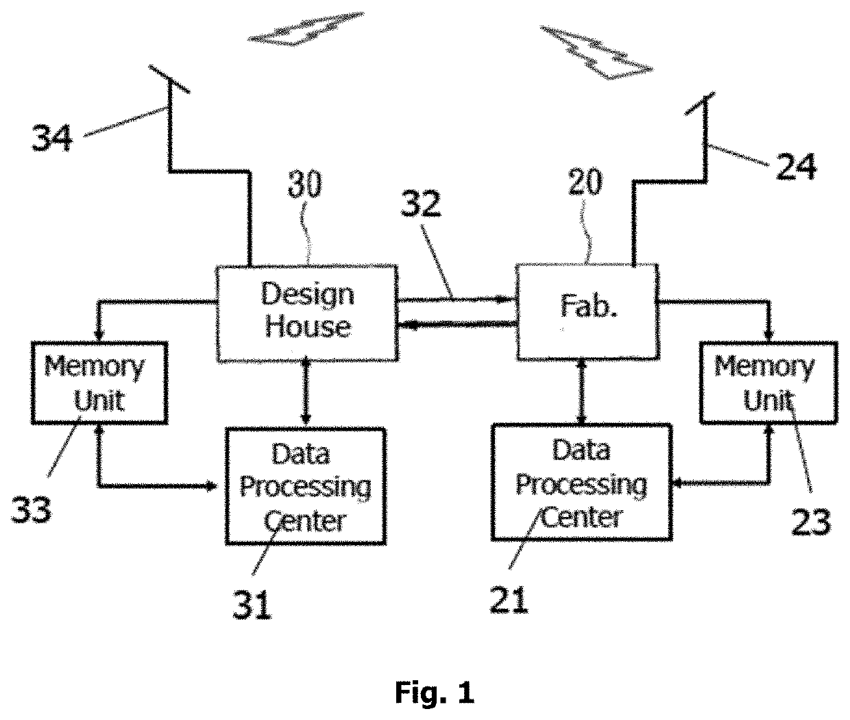
[0085]In semiconductor Fab, semiconductor assembly Fab, flat panel displayFab, solar cell Fab, printed circuit board Fab, mask Fab, LED Fab or LED assembly, Fab must process mask, lithography, etching, and film deposition, etc. equipment tools and run process to produce functional products. Because too many complex manufacturing, process and equipment parameter control and deviation, material control, or technical bottleneck will create many defects that affect product yield. Those defects cannot be avoided. So, semiconductor Fab will execute defect inspection in the manufacturing process to improve yield and reduce cost.

[0086]Besides, this invention's “Semiconductor Fab's Defect Operating System” include: Apply to IC design house and semiconductor fan, IC design house and semiconductor assembly Fab, IC design house and printed circuit board Fab, IC design house and mask Fab, IC design house and flat panel display Fab, IC design house and solar celly Fab, IC design house and LED Fab...


PUM


Abstract

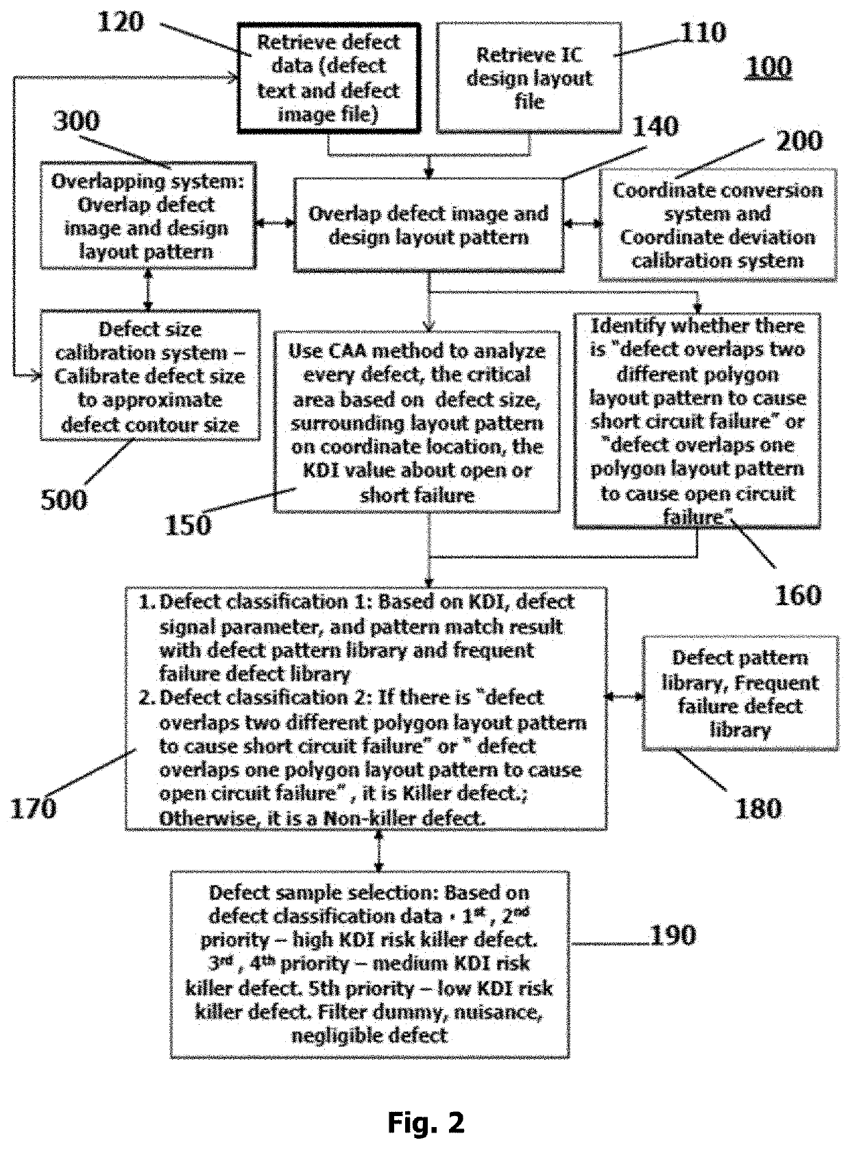
The present invention relates to “an Innovative Semiconductor Fab's Defect Operating System” thereof for design house and manufacturing Fab is provided. The Innovative Semiconductor Fab's Defect Operating System comprises: receiving pluralities of defect data, IC design layout data; analyzing the defect data, design layouts, by a Critical Area Analysis (CAA) method via a Defect Operating System located inside the Fab site; identify a killer or non-killer defect based on the open or short failure probability; sending the killer defect data to the design house via internet, FTP, etc. The design house receives the wafer testing yield data; pick the bad die information and the killer defect information for failure analysis; correlate the corresponding defect data with the wafer test data; sending the failure killer defect data to the Fab via internet, FTP, etc.; and improve the wafer yield through feed forward defect data and feedback of failure killer defect data which is an innovative “Defect Operation Platform” implementation between design house and Fab.

Description

BACKGROUND OF THE INVENTION1. Field of the Invention[0001]The present invention relates to “an Innovative Semiconductor Fab's Defect Operating System” that is used from the wafer manufacture to functional chips in a semiconductor Fab thereof for design house and manufacturing Fab is provided. Especially, this Semiconductor Fab's Defect Operating System can be applied to IC design house and semiconductor manufacturing Fab, IC design house and semiconductor assembly Fab, IC design house and PCB Fab, IC design house and mask manufacturing Fab, design house and flat panel display manufacturing Fab, design house and solar cell manufacturing Fab, and design house and LED manufacturing or assembly Fab.2. Description of the Prior Art[0002]In general, an integrated circuit design house or IC design house finish functional circuit design. Then, IC design house needs to authorize semiconductor Fab to manufacture based on the IC design layout designed by IC design house. Obviously, IC design ho...

Claims


Application Information

Patent Timeline
IPC IPC(8): G06F17/50
CPCG06F30/398G06F2119/22
Inventor LEU, IYUNTSAY, RAY JENN
Owner ELITETECH TECH
Why Eureka
Try Eureka