

Semiconducting co-polymers of methylenedihydropyrazines with fused thiophenes
- Summary
- Abstract
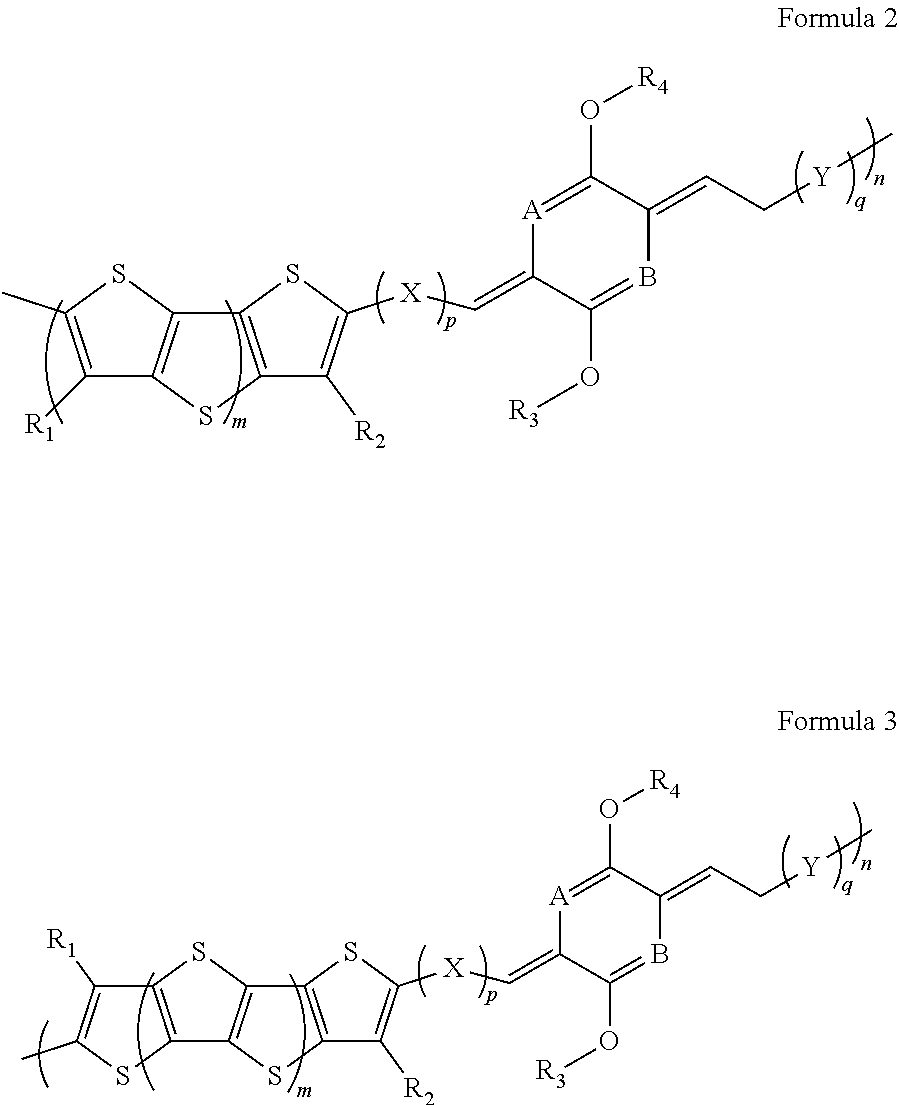
- Description
- Claims
- Application Information
AI Technical Summary
Benefits of technology
Problems solved by technology
Method used
Image

Examples
example 1
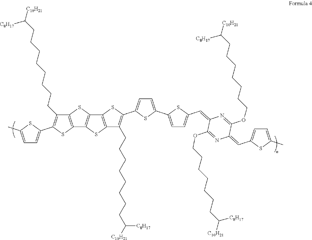
Preparation of AMDHP Fused-Thiophene Organic Semiconductor Polymer
[0098]The synthesis of the compound of Formula 4 was prepared according to Reaction Scheme 3 (shown below) where a tin-substituted dialkylated tetrathienoacene was reacted with a halogen-substituted thienyl-AMDHP.
[0099]Monomer A (tin-substituted-thienyl dialkylated tetrathienoacene) was synthesized using the following procedure. To a 100 mL flask, DTh Branched FT4 (2.3 g, 2.0 mmol, 1.0 eq.) and DCM (25 mL) were added under nitrogen protection. The reaction solution was cooled to 0° C. to 5° C. N-Bromosuccinimide (NBS) (0.72 g, 4.04 mmol, 2.02 eq.) was added in several small portions into the flask making sure that the reaction solution stayed below 10° C. The reaction mixture was stirred for 2 hrs below 10° C. HPLC analysis confirmed the completed reaction. Methylene chloride was removed under reduced pressure at 30° C. Hexane (20 mL) was added, and the resulting slurry was passed through a silica gel column eluting w...
example 2
Preparation of Devices with AMDHP Fused-Thiophene Organic Semiconductor Polymer
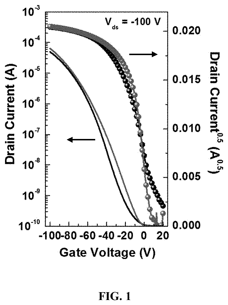
[0107]In some examples, a device having the AMDHP fused-thiophene organic semiconductor polymer described herein may be an electronic, optoelectronic, or nonlinear optical device, such as field-effect transistors (FET), thin-film transistors (TFT), organic light-emitting diodes (OLED), electro-optic (EO) devices, conductive materials, two photon mixing materials, organic semiconductors, RFID tags, electroluminescent devices, or photovoltaic and sensor devices.
[0108]In some examples, an organic thin film transistor (OTFT) includes a substrate; a gate electrode over the substrate; a gate dielectric layer over the substrate; a patterned source and drain layer over the gate dielectric layer; an organic semiconductor (OSC) layer over the gate dielectric layer; and, optionally, an insulator layer over the patterned source and drain layer, such that the OSC layer comprises the polymer having the composition of F...
PUM
| Property | Measurement | Unit |
|---|---|---|
| Mass | aaaaa | aaaaa |
| Mass | aaaaa | aaaaa |
| Temperature | aaaaa | aaaaa |
Abstract
Description
Claims
Application Information