

Thermosetting iodine- and silicon-containing material, composition containing the material for forming resist underlayer film for EUV lithography, and patterning process
- Summary
- Abstract
- Description
- Claims
- Application Information
AI Technical Summary
Benefits of technology
Problems solved by technology
Method used
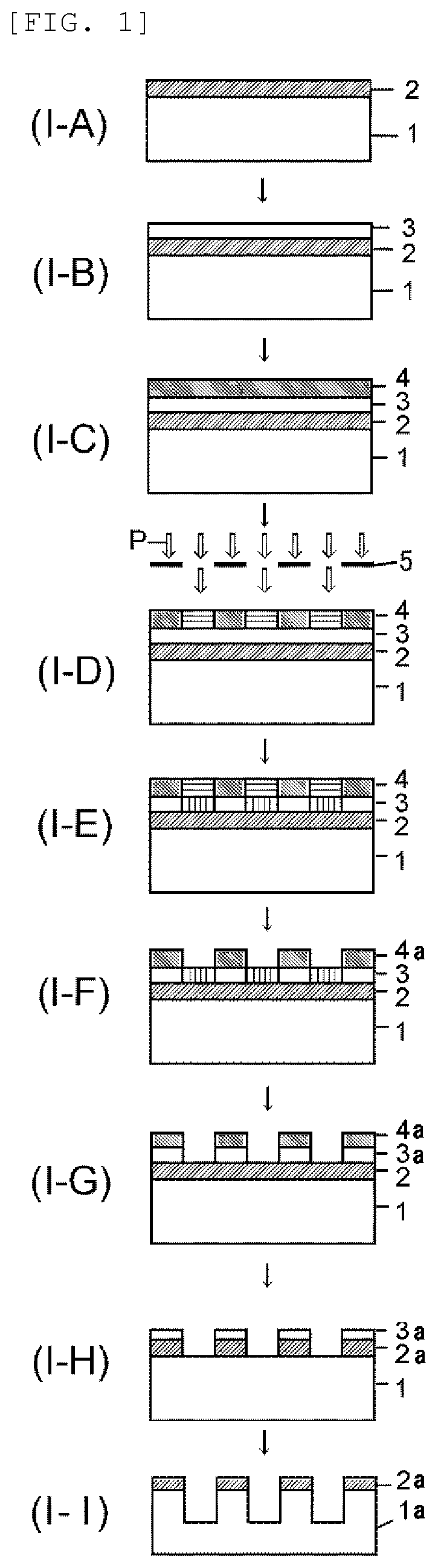
Image


Examples
synthesis example 1
[0222]To a mixture containing 120 g of methanol, 0.1 g of 10% nitric acid, and 60 g of deionized water, a mixture containing 19.8 g of Monomer 100, 13.6 g of Monomer 101, 22.8 g of Monomer 102, and 48.6 g of Monomer 110 was added and maintained at 40° C. for 12 hours to perform hydrolysis condensation. After completion of the reaction, 400 g of propylene glycol monoethyl ether (PGEE) was added thereto. Then, the water used for the hydrolysis condensation and by-produced alcohol were distilled off under reduced pressure. Thus, 450 g of PGEE solution of Iodine-Containing Polysiloxane Compound 1 was obtained (compound concentration: 20%). The molecular weight thereof was measured in terms of polystyrene and found Mw=2,500.
[0223][Synthesis Example 2] to [Synthesis Example 27] were carried out under the same conditions as in Synthesis Example 1 by using monomers shown in Table 1-1 and Table 1-2 to obtain the target products.
synthesis example 28
[0224]To a mixture containing 120 g of methanol, 0.1 g of 10% nitric acid, and 60 g of deionized water, a mixture containing 61.3 g of Monomer 101 and 12.9 g of Monomer 130 was added and maintained at 40° C. for 12 hours to perform hydrolysis condensation. After completion of the reaction, 300 g of propylene glycol monoethyl ether (PGEE) was added thereto. Then, the water used for the hydrolysis condensation and by-produced alcohol were distilled off under reduced pressure. Thus, 250 g of PGEE solution of Ammonium Salt-Containing Polysiloxane Compound 28 (Z-1) was obtained (compound concentration: 20%). The molecular weight thereof was measured in terms of polystyrene and found Mw=1,500.
TABLE 1-1SynthesisExampleRaw materials for reactionMw1Monomer 100: 19.8 g, Monomer 101: 13.6 g,2500Monomer 102: 22.8 g, Monomer 110: 48.6 g2Monomer 100: 19.8 g, Monomer 101: 13.6 g,2100Monomer 102: 30.4 g, Monomer 111: 35.2 g3Monomer 100: 19.8 g, Monomer 101: 13.6 g,2700Monomer 102: 38.1 g, Monomer 1...
PUM
| Property | Measurement | Unit |
|---|---|---|
| Length | aaaaa | aaaaa |
| Length | aaaaa | aaaaa |
| Length | aaaaa | aaaaa |
Abstract
Description
Claims
Application Information