SILICON METAL-OXIDE-SEMICONDUCTOR FIELD EFFECT TRANSISTOR (Si MOSFET) WITH A WIDE-BANDGAP III-V COMPOUND SEMICONDUCTOR GROUP DRAIN AND METHOD FOR FABRICATING THE SAME

a field effect transistor and silicon metal oxidesemiconductor technology, applied in the direction of transistors, semiconductor devices, electrical appliances, etc., can solve the problems of high signal loss of external power amplifiers/switchers via boards/packages, insufficient power/range handling capability, and high dynamic operation. , to achieve the effect of low breakdown voltage problem, high epitaxial quality, and low cos

Active Publication Date: 2021-05-27
NAT YANG MING CHIAO TUNG UNIV +1
View PDF0 Cites 1 Cited by
  • Summary
  • Abstract
  • Description
  • Claims
  • Application Information

AI Technical Summary

Benefits of technology

[0006]To overcome the abovementioned problems, the present invention provides a silicon metal-oxide-semiconductor field effect transistor with a wide-bandgap III-V compound material drain and a method for fabricating the same, which selectively grows III-V compound materials only in the opened MOSFET drain area with etched and exposed Si (111) facet on a Si (100) substrate for standard CMOS fabrication, there

Problems solved by technology

However, scaling down also constraints device's dynamic operation range and power handling capabilities.
However, when telecommunications (5G/6G) must use higher microwave and/or millimeter-wave frequencies for wider bandwidths and higher data rates, this technology will no longer be cost/performance-effective.
In the millimeter-wave radio/radar band, the signal loss of the external power amplifier/switch via board/package will be too high to meet the stringent system requirem

Method used


Image

  • SILICON METAL-OXIDE-SEMICONDUCTOR FIELD EFFECT TRANSISTOR (Si MOSFET) WITH A WIDE-BANDGAP III-V COMPOUND SEMICONDUCTOR GROUP DRAIN AND METHOD FOR FABRICATING THE SAME
  • SILICON METAL-OXIDE-SEMICONDUCTOR FIELD EFFECT TRANSISTOR (Si MOSFET) WITH A WIDE-BANDGAP III-V COMPOUND SEMICONDUCTOR GROUP DRAIN AND METHOD FOR FABRICATING THE SAME
  • SILICON METAL-OXIDE-SEMICONDUCTOR FIELD EFFECT TRANSISTOR (Si MOSFET) WITH A WIDE-BANDGAP III-V COMPOUND SEMICONDUCTOR GROUP DRAIN AND METHOD FOR FABRICATING THE SAME

Examples


Embodiment Construction

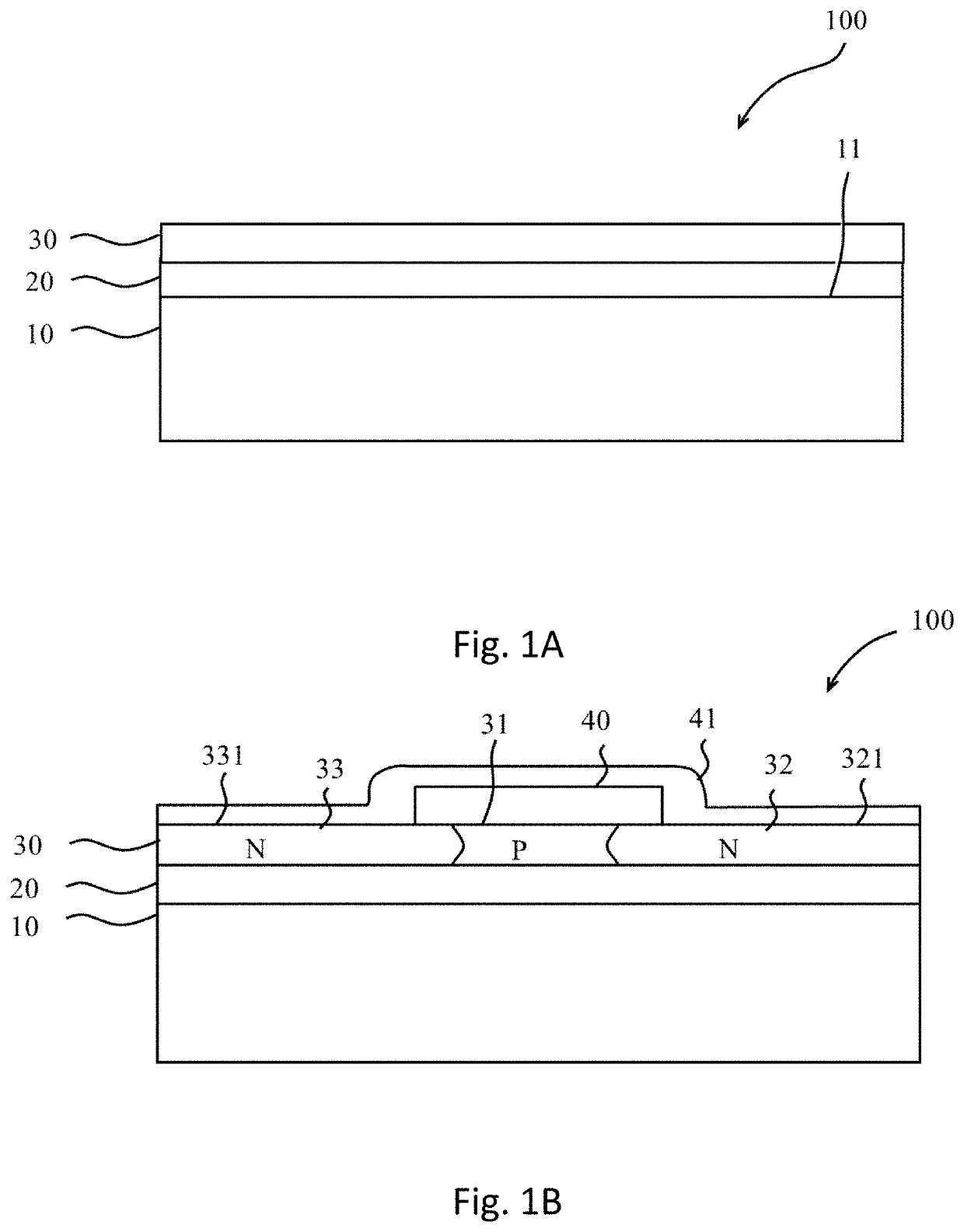
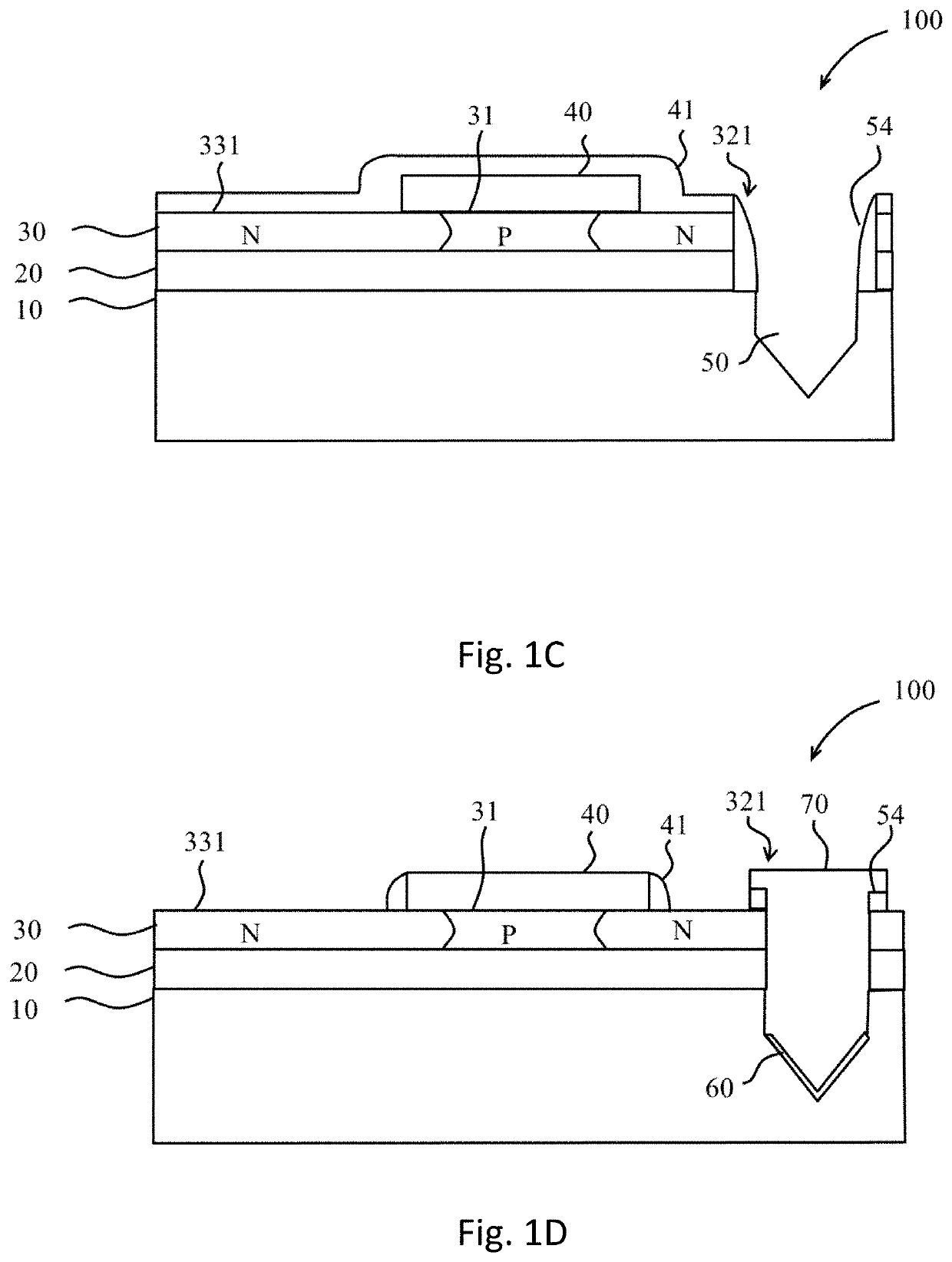
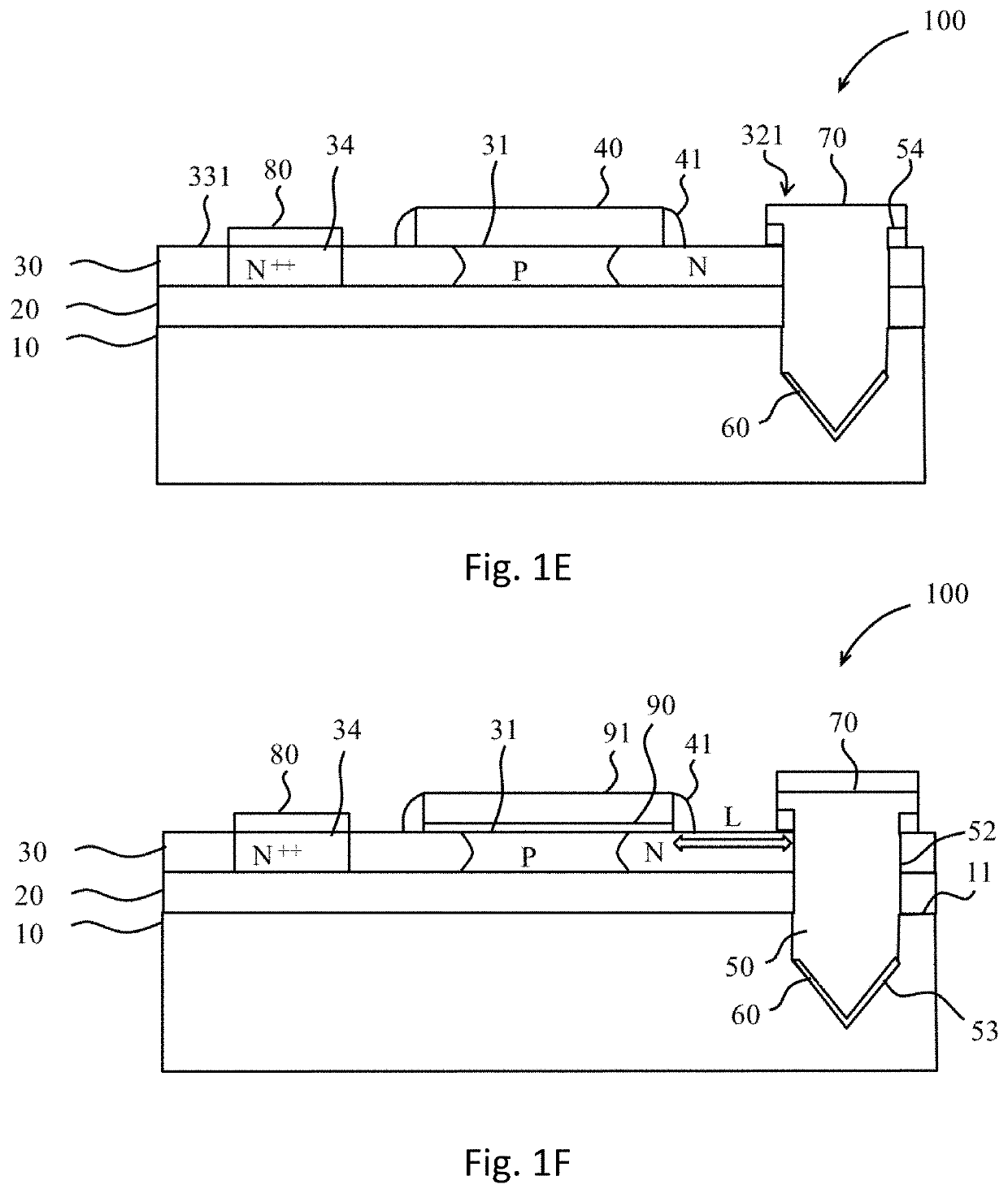
"d_n">[0017]The present invention provides a silicon metal-oxide-semiconductor field effect transistor with a wide-bandgap III-V compound material (for instance GaN) drain and a method for fabricating the same. The following embodiment is exemplified by a GaN drain fabricated on a silicon-on-insulator (SOI) substrate, but the present invention is not limited thereto. Refer to FIGS. 1A-1F, which are diagrams schematically illustrating the steps of fabricating a silicon metal-oxide-semiconductor field effect transistor (MOSFET) with a GaN drain according to an embodiment of the present invention. The method comprises the steps:

[0018]As shown in FIG. 1A, a substrate 100 is firstly provided. In the embodiment, the substrate 100 is exemplified by a SOI substrate. The substrate 100 comprises a silicon substrate 10, an insulation layer 20, and a semiconductor layer 30. The silicon substrate 10 has a (100) facet as a main surface 11, the insulation layer 20 is formed on the main surface 11,...


PUM


Abstract

A silicon metal-oxide-semiconductor field effect transistor with a wide-bandgap III-V compound semiconductor drain and a method for fabricating the same are disclosed. The method fabricates a hundred nanometer-scale hole in a (100) silicon substrate to expose the (111) facet of the silicon substrate, which favors to use selective area growth to form lattice matched III-V materials with high quality.

Description

[0001]This application claims priority for Taiwan patent application no. 108142879 filed on 26 Nov. 2019, the content of which is incorporated by reference in its entirely.BACKGROUND OF THE INVENTIONField of the Invention[0002]The present invention relates to a heterogeneously integrated silicon metal-oxide-semiconductor field effect transistor, particularly to a silicon metal-oxide-semiconductor field effect transistor with a wide-bandgap III-V compound semiconductor (for instance, 3.4 eV for GaN versus 1.1 eV for Si) drain and a method for fabricating the same.Description of the Related Art[0003]The III-V compound semiconductors, such as gallium nitride (GaN) material, have many unique physical characteristics, such as wide energy gap (3.4 eV) between the material's valence and conduction bands, low electron impact ionization coefficient (<1×10⁻⁶ versus that of Silicon) leading to high breakdown voltage, high electron drift velocity, etc. Thus, the wide-bandgap III-V compound s...

Claims


Application Information

Patent Timeline
IPC IPC(8): H01L29/78H01L29/06H01L29/04H01L29/08H01L29/66H01L29/267
CPCH01L29/7833H01L29/0653H01L29/0676H01L29/04H01L29/0847H01L29/2003H01L29/66522H01L29/66492H01L29/267H01L29/66545H01L29/66636H01L29/78H01L29/66568H01L21/02639H01L21/0254H01L21/02381H01L21/02433H01L21/0243H01L21/02458H01L21/0262H01L21/02598H01L21/30608H01L29/78618H01L29/42384H01L29/7869H01L29/66969H01L21/30604H01L29/16
Inventor CHANG, EDWARD YICHANG, MAU-CHUNG FRANKCHUANG, CHIEH-HSILIN, JESSIE
Owner NAT YANG MING CHIAO TUNG UNIV
Why Eureka
Try Eureka