Multijunction solar cells

a solar cell and multi-junction technology, applied in the field of solar cells and the fabrication of solar cells, can solve the problems of increasing the complexity of properly specifying and manufacturing, affecting the current collection of the active layer, and unable to meet the requirements of solar cell arrays, etc., to achieve enhanced hole-electron pairs, improved current collection in the active layer, and enhanced hole-electron pair generation

Active Publication Date: 2021-11-11
SOLAERO TECH CORP
View PDF4 Cites 1 Cited by
  • Summary
  • Abstract
  • Description
  • Claims
  • Application Information

AI Technical Summary

Benefits of technology

[0057]In some embodiments, the generation of hole-electron pairs is enhanced in certain regions of the active layer due to a change in band gap in regions of the active layer.
[0058]In some embodiments, the band gap decrease from the top surface of the one subcell t

Problems solved by technology

Compared to silicon, III-V compound semiconductor multijunction devices have greater energy conversion efficiencies and generally more radiation resistance, although they tend to be more complex to properly specify and manufacture.
Such rigorous testing and qualifications are not generally applicable to terrestrial solar cells and solar cell arrays.
The space solar cells and arrays experience a variety of complex environments in space missions, including the vastly different illumination levels and temperatures seen during normal earth orbiting missions, as well as even more challenging environments for deep space missions, operating at different distances from the sun, such as at 0.7, 1.0 and 3.0AU (AU meaning astronomical units).
The photovoltaic arrays also endure anomalous events from space environmental conditions, and unforeseen environmental interactions during exploration missions.
Hence, electron and proton radiation exposure, collisions with space debris, and/or normal aging in the photovoltaic array and other systems could cause suboptimal operating conditions that degrade the overall power system performance, and may result in failures of one or more solar cells or array strings and consequent loss of power.
Such precautions are generally unnecessary in terrestrial applications.
In summary, it is evident that the differences in design, materials, and configurations between a space-qualified III-V compound semiconductor solar cell and subassemblies and arrays of such solar cells, on the one hand, and silicon solar cells or other photovoltaic devices used in terrestrial applications, on the other hand, are so substantial that prior teachings associated with silicon or other terrestrial photovoltaic system are simply unsuitable and have no applicability to the design configuration of space-qualified solar cells and arrays.
Charged particles in space could lead to damage to solar cell structures, and in some cases, dangerously high voltage being established across individual devices or conductors in the solar array.
These large voltages can lead to catastrophic electrostatic discharging (ESD) events.
However, in reality, changing a material parameter that increases the voltage may result in a decrease in current, and therefore a lower power output.
Such material design parameters are interdependent and interact in complex and often unpredictable ways, and for that reason are not “result effect

Method used


Image

  • Multijunction solar cells
  • Multijunction solar cells
  • Multijunction solar cells

Examples


first embodiment

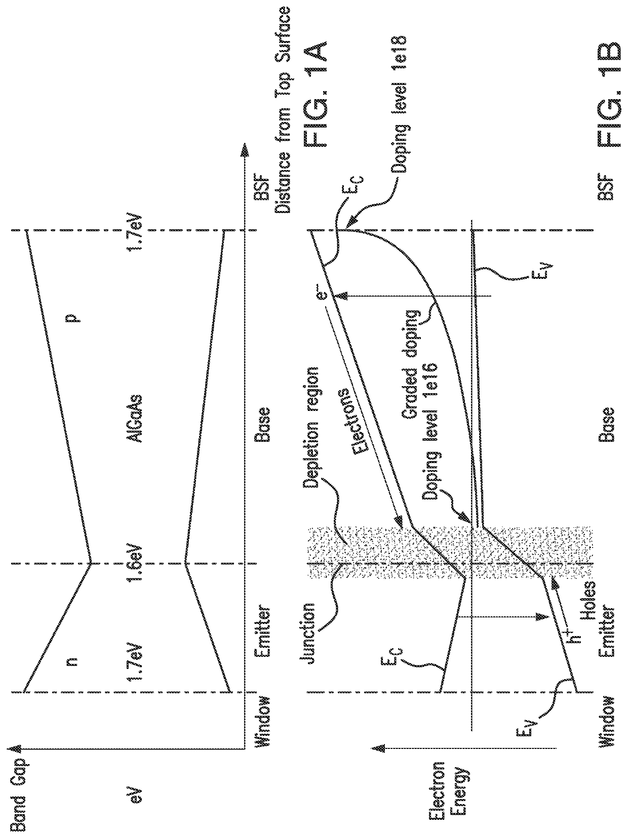
[0128]FIG. 1A is a graph of the band gap throughout the thickness of a solar subcell, according to the present disclosure.

[0129]FIG. 1B is a cross-sectional view of the solar subcell of FIG. 1A depicting the movement of electrons and holes throughout the thickness of the layer due to the internal electric field. The conduction Ec and the valence Ev bands are illustrated, as well as the emitter and base regions of the solar subcell, the junction, the depletion region, and graded doping throughout the thickness of the subcell.

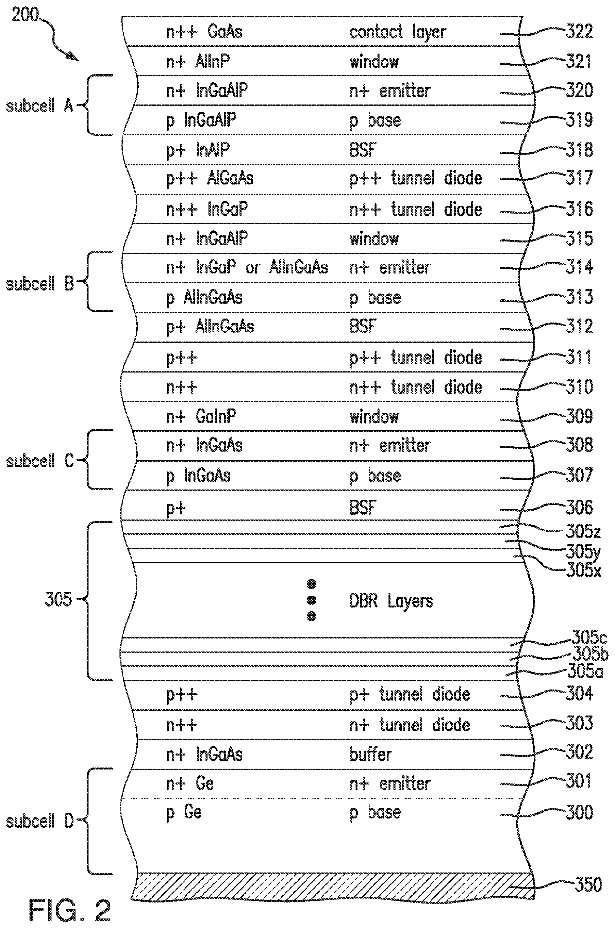
[0130]To illustrate an embodiment of a multijunction solar cell device of the present disclosure, FIG. 2 is a cross-sectional view of an embodiment of a four junction solar cell 200 after several stages of fabrication including the growth of certain semiconductor layers on the growth substrate up to the contact layer 322 according to the present disclosure.

[0131]As shown in the illustrated example of FIG. 2, the bottom subcell D includes a growth substrate 300 fo...

second embodiment

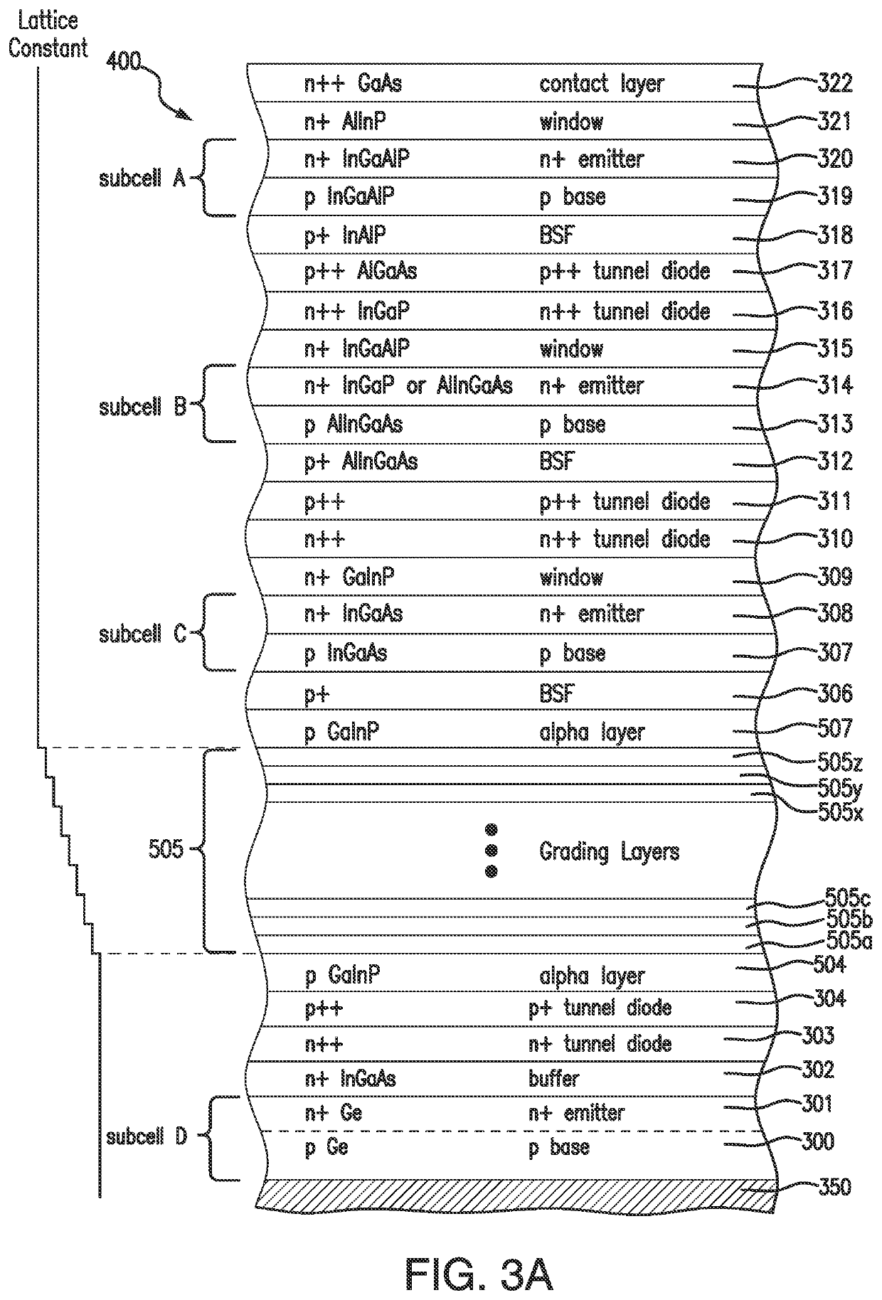
[0150]FIG. 3A is a cross-sectional view of a four junction solar cell 400 after several stages of fabrication including the growth of certain semiconductor layers on the growth substrate up to the contact layer 322, with various subcells being similar to the structure described and depicted in FIG. 2. In the interest of brevity, the description of layers 350, 300 to 304, and 306 through 322 will not be repeated here.

[0151]In the embodiment depicted in FIG. 3A, an intermediate graded interlayer 505, comprising in one embodiment step-graded sublayers 505a through 505z, is disposed over the tunnel diode layer 304. In particular, the graded interlayer provides a transition in lattice constant from the lattice constant of the substrate to the larger lattice constant of the middle and upper subcells.

[0152]The graph on the left side of FIG. 3A depicts the in-plane lattice constant being incrementally monotonically increased from sublayer 505a through sublayer 505z, such sublayers being ful...

third embodiment

[0162]In the third embodiment depicted in FIG. 3B, an intermediate graded interlayer 505, comprising in one embodiment step-graded sublayers 505a through 505zz, is disposed over the tunnel diode layer 304. In particular, the graded interlayer provides a transition in lattice constant from the lattice constant of the substrate to the larger lattice constant of the middle and upper subcells, and differs from that of the embodiment of FIG. 3A only in that the top or uppermost sublayer 505zz of the graded interlayer 506 is strained or only partially relaxed, and has a lattice constant which is greater than that of the layer above it, i.e., the alpha layer 506 (should there be a second alpha layer) or the BSF layer 306. In short, in this embodiment, there is an “overshoot” of the last one sublayer 505zz of the grading sublayers, as depicted on the left hand side of FIG. 4B, which shows the step-grading of the lattice constant becoming larger from layer 505a to 505zz, and then decreasing ...


PUM


Abstract

A multijunction solar cell including an upper first solar subcell having a first band gap and positioned for receiving an incoming light beam; a second solar subcell disposed below and adjacent to and lattice matched with said upper first solar subcell, and having a second band gap smaller than said first band gap; wherein at least one of the solar cells has a graded band gap throughout its thickness.

Description

REFERENCE TO RELATED APPLICATIONS[0001]The present application claims the benefit of U.S. Provisional Patent Application Ser. No. 62 / 948,451 filed Dec. 16, 2019. The present application is related to U.S. patent application Ser. No. 15 / 681,144 filed Aug. 18, 2017, which is a continuation-in-part of Ser. No. 14 / 828,206 filed Aug. 17, 2015.[0002]This application is related to co-pending U.S. patent application Ser. No. 14 / 660,092 filed Mar. 17, 2015, which is a division of U.S. patent application Ser. No. 12 / 716,814 filed Mar. 3, 2010, now U.S. Pat. No. 9,018,521; which is a continuation in part of U.S. patent application Ser. No. 12 / 337,043 filed Dec. 17, 2008.[0003]This application is also related to U.S. patent application Ser. No. 16 / 667,687 filed Oct. 29, 2019 which is a division of Ser. No. 13 / 872,663 filed Apr. 29, 2012, now U.S. Pat. No. 10,541,349, which was also a continuation-in-part of application Ser. No. 12 / 337,043, filed Dec. 17, 2008.[0004]This application is also rela...

Claims


Application Information

Patent Timeline
IPC IPC(8): H01L31/0725H01L31/0735H01L31/18
CPCH01L31/0725H01L31/1892H01L31/1844H01L31/0735Y02E10/544H01L31/06875H01L31/065H01L31/0687H01L31/0549Y02E10/52Y02P70/50
Inventor DERKACS, DANIELHART, JOHNBITTNER, ZACHARY
Owner SOLAERO TECH CORP
Why Eureka
Try Eureka