Method of manufacturing semiconductor device

a manufacturing method and semiconductor technology, applied in semiconductor devices, instruments, electrical devices, etc., can solve the problems of increasing power consumption, affecting the function of switching elements, and shifting the threshold voltage of a tft to the positive or negative sid

Inactive Publication Date: 2000-11-28
SEMICON ENERGY LAB CO LTD
View PDF22 Cites 89 Cited by
  • Summary
  • Abstract
  • Description
  • Claims
  • Application Information

AI Technical Summary

Benefits of technology

As a result, a chemical equilibrium state for the impurity element is established between the processing atmosphere and the surface to be processed. With this measure, the chemical reaction involving the impurity element near the surface of the silicon film can be suppressed, whereby the impurity element for threshold voltage control can effectively be prevented from being removed from the silicon film.

Problems solved by technology

However, there may occur an event that the threshold voltage of a TFT shifts to the positive or negative side due to indefinite factors in a manufacturing process, such as influences of mobile ions that have been introduced by pollution and a difference in work function or interface charge in the vicinity of the gate of the TFT.
Such a shift of the threshold voltage causes adverse effects such as impairing the switching element function and increasing the power consumption.
Although the pollution-induced factors can be removed by, for instance, improving the process, the factors caused by a work function difference or the like are determined by the materials used and hence are difficult to remove in some cases.
However, in experimentally producing various kinds of TFTs by using crystalline silicon films of the above kind, the present inventors have found that a serious problem occurs in applying the above-mentioned channel doping.
Since the concentration of the impurity element in the region (in the vicinity of the surface of the active layer) where a channel is to be formed is much reduced, the intended effect of the channel doping is not obtained, which makes it impossible to control the threshold voltage precisely.

Method used


Image

  • Method of manufacturing semiconductor device
  • Method of manufacturing semiconductor device
  • Method of manufacturing semiconductor device

Examples


embodiment 2

This embodiment is directed to a case where the invention is applied to a high-temperature polysilicon technique. Although for simplicity the following description is directed to a case of forming an n-channel TFT, the present invention can easily be applied to a known single-gate CMOS circuit and dual-gate CMOS circuit.

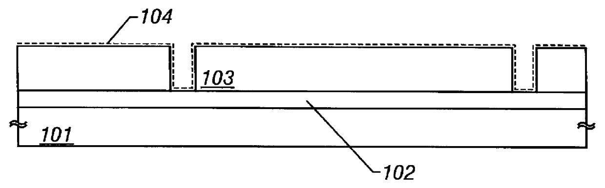
In FIG. 4A, reference numerals 401 and 402 denote a quartz substrate and a crystalline silicon film as an active layer, respectively. The crystalline silicon film 402 is obtained by crystallizing an amorphous silicon film by a heat treatment of 600.degree. C. for 24-48 hours. In this embodiment, naturally boron as an impurity element for threshold voltage control is added in forming the amorphous silicon film.

Next, a heat treatment is performed at 1,000.degree. C. for 30 minutes in an oxygen atmosphere containing hydrogen chloride and diborane at 3% and 7%, respectively. As a result, a 50-nm-thick thermal oxidation film 403 to later serve as a gate insulating film (s...

embodiment 3

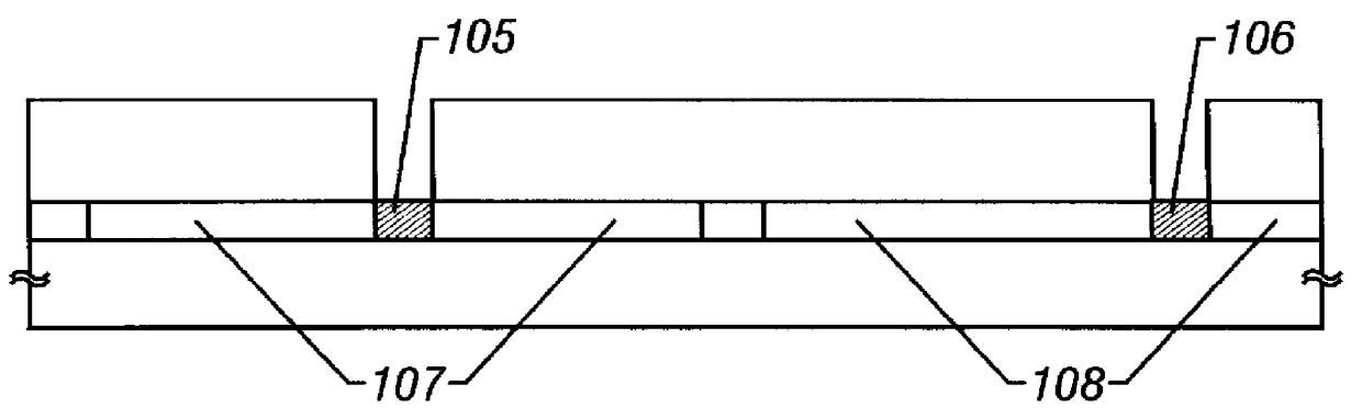
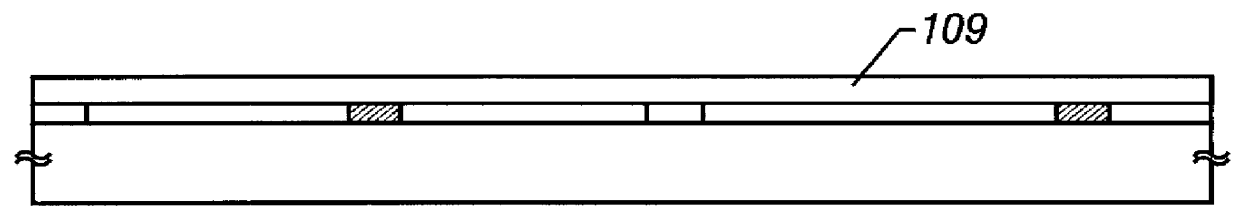
While the first and second embodiments are directed to the case of introducing boron by using diborane as one of the gases for forming an amorphous silicon film, B ions may be added by ion implantation or plasma doping without mass separation.

In the latter case, it is desirable that B ions be added before the crystallization step because the implantation of ions into a crystalline silicon film returns it to an amorphous state. By using a mask, B ions may be added selectively, i.e., only to a region that will become a channel forming region.

embodiment 4

The present invention can be applied to various electro-optical devices. For example, an active matrix liquid crystal display device can be constructed by inserting and holding a liquid crystal between the active matrix substrate of the first embodiment and an opposed substrate. In this case, a transmission-type liquid crystal display device is obtained if the pixel electrodes are formed by using a transparent material, and a reflection-type liquid crystal display device is obtained if they are formed by using a light-reflective material.

Further, an active matrix EL display device, an active matrix EC display device, or the like can easily be manufactured by somewhat changing the configuration of the active matrix substrate.


PUM

PropertyMeasurementUnit
thicknessaaaaaaaaaa
thicknessaaaaaaaaaa
thicknessaaaaaaaaaa

Abstract

A catalyst element for accelerating crystallization is added to an amorphous silicon film containing an impurity element for threshold voltage control, and a heat treatment is then performed to obtain a crystalline silicon film. Thereafter, the catalyst element is gettered by performing a heat treatment in an atmosphere containing a halogen element. In this step, a chemical equilibrium state is established for the impurity element for threshold voltage control by mixing a compound gas containing the impurity element into the atmosphere, thereby preventing the impurity element from escaping into the vapor phase.

Description

1. Field of the InventionThe present invention relates to a method of manufacturing a semiconductor device that uses a thin-film semiconductor having crystallinity. In particular, the invention relates to manufacture of an insulated-gate thin-film transistor (TFT).2. Description of the Related ArtIn recent years, the techniques of forming a TFT using a crystalline silicon film (particularly a film made of a material called polysilicon film) on a substrate having an insulative surface have been developed. A TFT using such a material is advantageous over a TFT using an amorphous silicon film in being capable of high-speed operation.For this reason, extensive studies are now being made on the monolithic panel in which a pixel matrix circuit and driver circuits are formed on the same substrate as well as the system-on-panel structure in which signal processing logic circuits (memories, amplifiers, a CPU, etc.) are additionally formed in an integral manner. For example, the driver circui...

Claims


Application Information

Patent Timeline
Patent Type & Authority Patents(United States)
IPC IPC(8): H01L21/02H01L29/66H01L21/70H01L21/336H01L27/12H01L29/786H01L21/84G02F1/13G02F1/1362H01L21/205H01L21/20H01L21/77
CPCH01L27/12H01L27/1277H01L29/78624H01L29/66757G02F1/13454
Inventor YAMAZAKI, SHUNPEIOHTANI, HISASHI
Owner SEMICON ENERGY LAB CO LTD
Why Eureka
Try Eureka