Spacer formation by poly stack dopant profile design

a technology of dopant profile and spacer, which is applied in the direction of transistors, electrical devices, semiconductor devices, etc., can solve the problems of permanent change of the threshold voltage of the device, and achieve the effects of less likely to fail, more reliable, and longer li

Inactive Publication Date: 2000-12-12
CONVERSANT INTPROP MANAGEMENT INC
View PDF8 Cites 9 Cited by
  • Summary
  • Abstract
  • Description
  • Claims
  • Application Information

AI Technical Summary

Benefits of technology

Advantageously, the dimensions of the silicon dioxide knob can be varied to form a graded channel having a different geometry. The steps are easily performed and one implantation for heavy doping is all that is needed to form the graded junction or doping pattern. The resulting device has a longer life, is more reliable and less likely to fail than devices without...

Problems solved by technology

Trapped charge in the gate insulator due to injected hot carriers accumulates ...

Method used


Image

  • Spacer formation by poly stack dopant profile design
  • Spacer formation by poly stack dopant profile design
  • Spacer formation by poly stack dopant profile design

Examples


Embodiment Construction

In the following detailed description of the preferred embodiments, reference is made to the accompanying drawings which form a part hereof, and in which are shown by way of illustration specific embodiments in which the invention may be practiced. It is to be understood that other embodiments may be utilized and structural changes may be made without departing from the scope of the present invention.

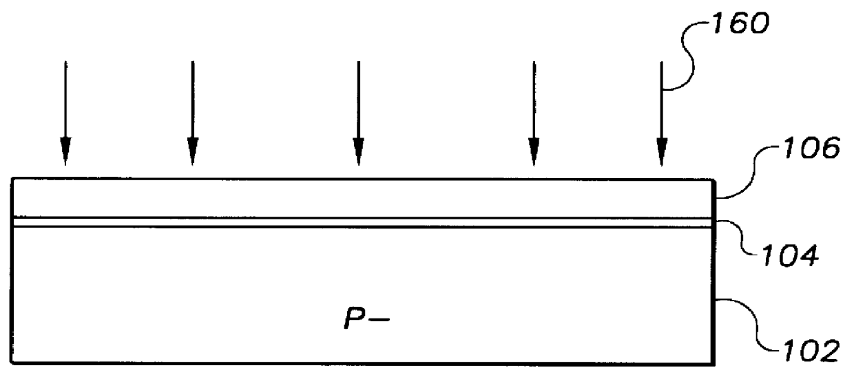
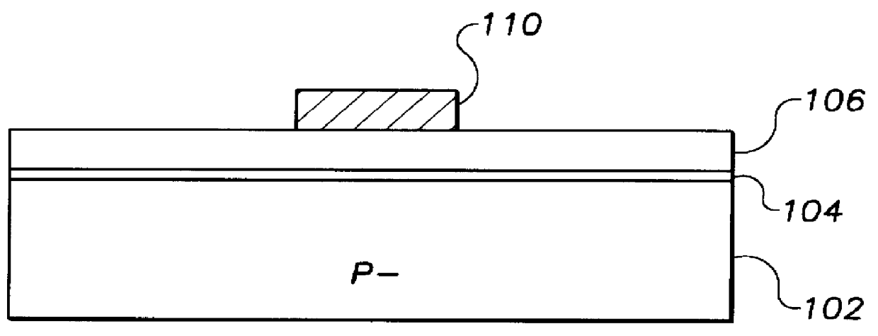
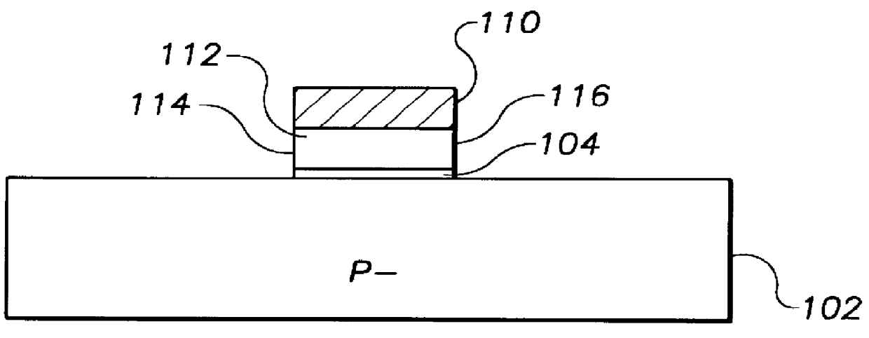
Described first is an NPN type transistor also known as an NMOSFET. In FIG. 1A, silicon substrate 102 suitable for integrated circuit manufacture includes P-type epitaxial layer with a boron background concentration on the order of 1.times.10.sup.6 atoms / cm.sup.3, a orientation and a resistivity of 12 ohm-cm. Preferably, the epitaxial surface layer is disposed on a P+ base layer (not shown) and includes a planar top surface. Gate oxide 104, composed of silicon dioxide (SiO2), is formed on the top surface of substrate 102 using oxide tube growth at a temperature of 700.degree. to 1000.d...


PUM


Abstract

A method for forming a semiconductor device to produce graded doping in the source region and the drain region includes the steps of implanting the gate material, usually a polysilicon, with a dopant ion that varies the level of oxide formation on the gate. The dopant ion is driven into undoped polysilicon. Nitrogen ions, may also be implanted in the polysilicon to contain the previously implanted ions. For N-type transistors, typically arsenic is implanted. For P-type transistors, typically boron is implanted. Gates are formed. The gate structure is then oxidized. The oxidation process is controlled to grow a desired thickness of silicon dioxide on the gate. The portion of the gate carrying the dopant grows silicon dioxide either more quickly or more slowly. An isotropic etch can then used to remove a portion of the silicon oxide and form a knob on each sidewall of the gate. A heavy ion implant is then done to convert a portion of the lightly doped source region into a heavily doped region within the source region, and to convert a portion of the lightly doped drain region into a heavily doped region within the drain region. Some of the implanted ions are stopped by the knobs on the gate sidewalls. The regions under the knobs do not have as deep an ion implantation resulting in a shallow region beneath the knob. This forms a graded junction having a specific geometry. The geometry of the interface between the lightly doped region and the heavily doped region in the source region and the drain region depends on the geometry (thickness) of silicon dioxide knobs formed on the sidewall of the gate.

Description

FIELD OF THE INVENTIONThe present invention relates generally to integrated circuit manufacturing and more particularly to forming insulated gate field effect transistors.BACKGROUND OF THE INVENTIONAn insulated-gate field-effect transistor (IGFET), such as a metal-oxide semiconductor field-effect transistor (MOSFET), uses a gate to control an underlying surface channel joining a source and a drain. The channel, source and drain are located in a semiconductor substrate, with the source and drain being doped oppositely to the substrate. The gate is separated from the semiconductor substrate by a thin insulating layer such as a gate oxide. The operation of the IGFET involves application of an input voltage to the gate, which sets up a transverse electric field in the channel in order to modulate the longitudinal conductance of the channel.In typical IGFET processing, the source and drain are formed by introducing dopants of second conductivity type (P or N) into a semiconductor substra...

Claims


Application Information

Patent Timeline
IPC IPC(8): H01L21/28H01L21/02H01L29/66H01L21/336H01L29/78
CPCH01L21/28052H01L21/28176H01L29/7833H01L29/6659H01L21/28211H01L29/66598
Inventor GARDNER, MARKHAUSE, FREDMAY, CHARLES
Owner CONVERSANT INTPROP MANAGEMENT INC
Why Eureka
Try Eureka