Nucleation and deposition of PT films using ultraviolet irradiation

Inactive Publication Date: 2001-03-20
MICRON TECH INC
View PDF9 Cites 115 Cited by
  • Summary
  • Abstract
  • Description
  • Claims
  • Application Information

AI Technical Summary

Problems solved by technology

Conventional methods of depositing platinum films suffer drawbacks in that these methods are unable to consistently create a continuous uniformly thin platinum film that additionally has good step coverage.
Even in the conventional chemical vapor deposition methods it is difficult to create a continuous uniform platinum film with good step coverage.
This is likely due to the fact that when conventional platinum precursors are used in the conventional chemical vapor deposition methods, it is difficult to control the nucleation rate of the platinum films.
At the outset of the platinum deposition process, the nucleation rate of the platinum film onto the surface of the substrate is very slow; however, once nucleation does begin the deposition rate of the platinum film onto the surface increases significantly.
In fact, it is difficult to control or even slow the rate of deposition once the conventional methods begin depositing platinum onto the surface of the substrate.
In the conventiona

Method used


Image

  • Nucleation and deposition of PT films using ultraviolet irradiation
  • Nucleation and deposition of PT films using ultraviolet irradiation
  • Nucleation and deposition of PT films using ultraviolet irradiation

Examples


Embodiment Construction

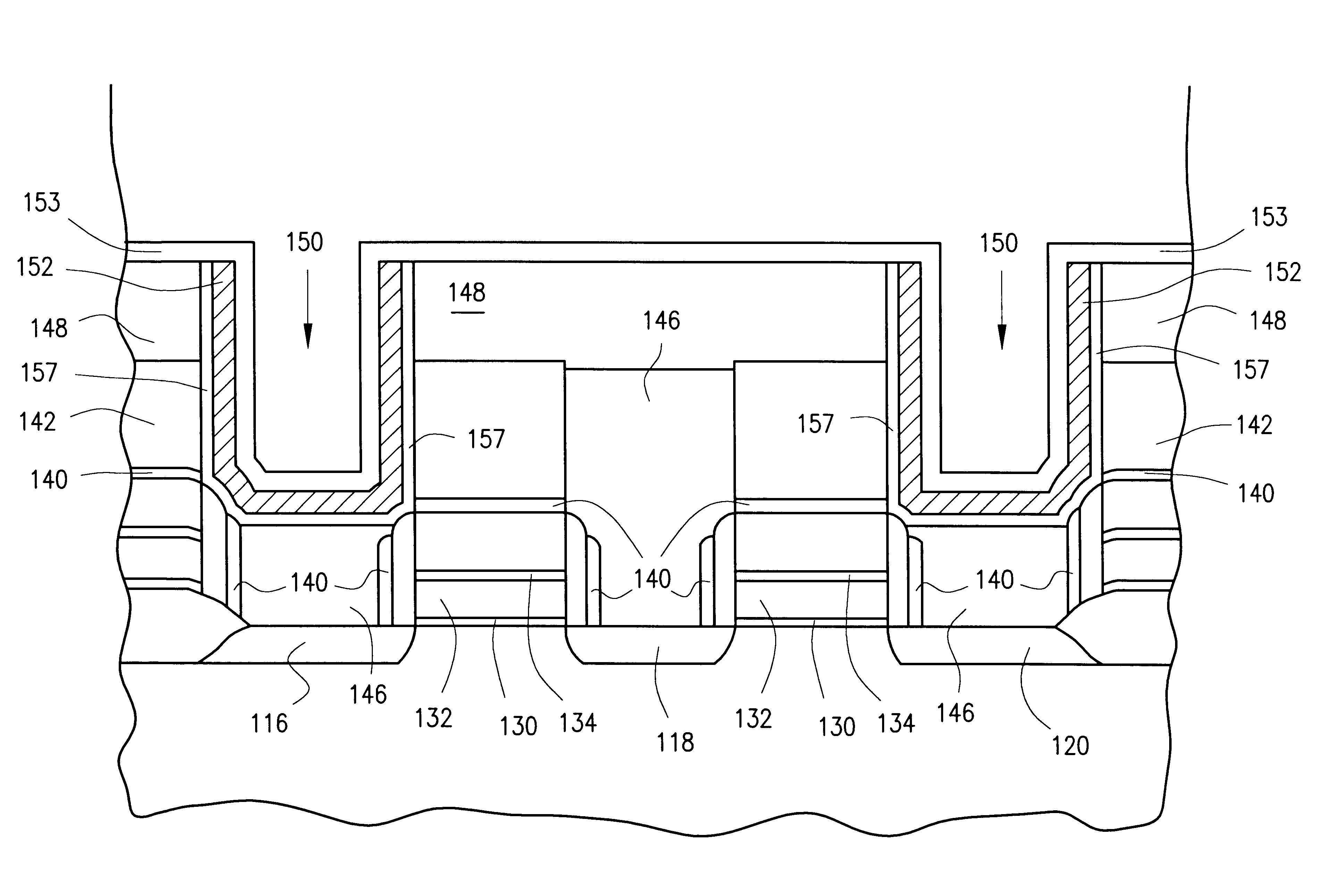
In this example a lower electrode for a capacitor in a memory cell is formed of platinum according to the present invention. Referring to FIG. 4, a semiconductor wafer fragment at an early processing step is indicated generally by reference numeral 100. The semiconductor wafer 100 is comprised of a bulk silicon substrate 112, which may be doped to a predetermined conductivity type, and with field isolation oxide regions 114 and active areas 116, 118, 120 formed therein. Word lines 122, 124, 126, 128 have been constructed on the wafer 100 in a conventional manner. Each word line consists of a lower gate oxide 130, a lower polysilicon layer 132, a higher conductivity silicide layer 134 and an insulating silicon nitride cap 136. Each word line has also been provided with sidewall insulating spacers 138, which are also composed of silicon nitride.

Referring now to FIG. 5, a thin layer 140 of nitride or TEOS (tetraethyl orthosilicate) is then provided atop the wafer 100. Next a layer of i...


PUM

PropertyMeasurementUnit
Timeaaaaaaaaaa
Timeaaaaaaaaaa
Thicknessaaaaaaaaaa

Abstract

A method of depositing a platinum based metal film by CVD deposition includes bubbling a non-reactive gas through an organic platinum based metal precursor to facilitate transport of precursor vapor to the chamber. The platinum based film is deposited onto a non-silicon bearing substrate in a CVD deposition chamber in the presence of ultraviolet light at a predetermined temperature and under a predetermined pressure. The film is then annealed in an oxygen atmosphere at a sufficiently low temperature to avoid oxidation of substrate. The resulting film is free of silicide and consistently smooth and has good step coverage.

Description

The invention relates generally to the chemical vapor deposition (CVD) of platinum group metals on an integrated circuit structure as a continuous film and with good step coverage. The invention also relates to integrated circuits having a platinum group metal layer, used, for example, as the lower electrode in a capacitor.DISCUSSION OF RELATED ARTBecause of their high corrosion resistance, microelectronic devices having platinum group metals are desired in applications where great reliability is desired and also where a corrosive atmosphere may be present. A process is needed to deposit a platinum group metal having good step coverage and where the platinum film can be patterned to avoid an extra etching step.Conventional methods of depositing platinum films suffer drawbacks in that these methods are unable to consistently create a continuous uniformly thin platinum film that additionally has good step coverage. These conventional prior methods include vacuum deposition methods, sp...

Claims


Application Information

Patent Timeline
IPC IPC(8): C23C16/48H01L21/02H01L21/285H01L21/70H01L21/768
CPCC23C16/482H01L21/28556H01L21/28568H01L21/7687H01L21/76877H01L28/60
Inventor MARSH, EUGENE P.
Owner MICRON TECH INC
Why Eureka
Try Eureka