Method of forming metal lands at the M0 level with a non selective chemistry

Inactive Publication Date: 2001-07-10
IBM CORP
View PDF10 Cites 13 Cited by
  • Summary
  • Abstract
  • Description
  • Claims
  • Application Information

AI Technical Summary

Benefits of technology

It is another object of the present invention to provide a method of forming metal lands at the M0 level with a non selective chemistry wherein the CB recess etching step is no longer necessary.
It is another object of the present invention to provide a method of forming metal lands at the M0 level with a non selective chemistry which eliminates oxide fen

Problems solved by technology

Unfortunately, the above-described two-step etch process is not satisfactory.
Tapered contact holes are a potential source of electrical shorts occurring between two adjacent M0 metal lands, in turn resulting in a high number of failed cells.
In addition, the chemistry of step 2 has different etch rates between ARC, polysilicon

Method used


Image

  • Method of forming metal lands at the M0 level with a non selective chemistry
  • Method of forming metal lands at the M0 level with a non selective chemistry
  • Method of forming metal lands at the M0 level with a non selective chemistry

Examples


Example

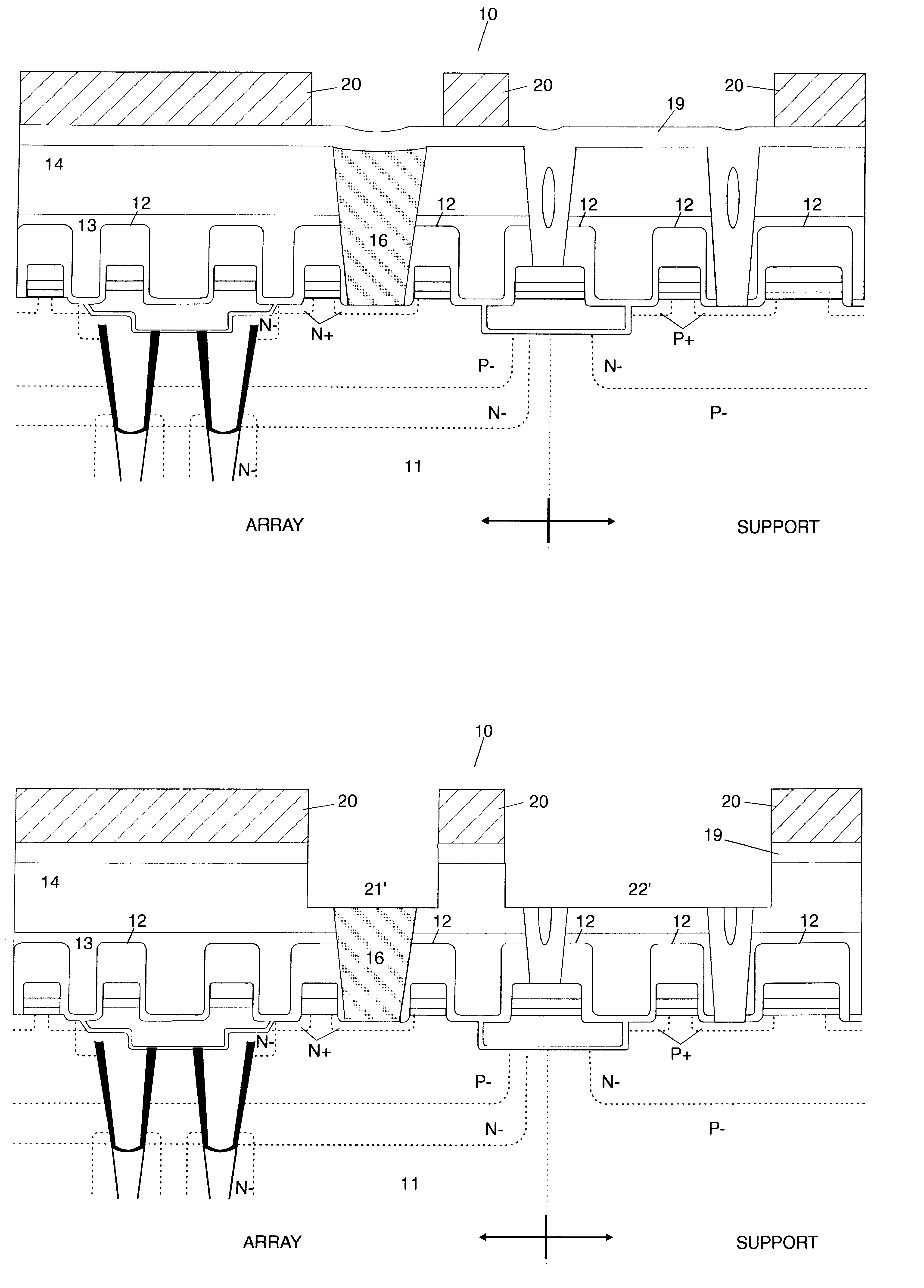
Applicant's inventor has discovered that the plasma etching process of the prior art method described above by reference to FIG. 1 and FIGS. 2A to 2E can be significantly improved. The essential point consists in an etching chemistry change which in turn requires some modifications in the above described operating conditions. An additional process optimization may be obtained thanks to a different wafer plasma environment.

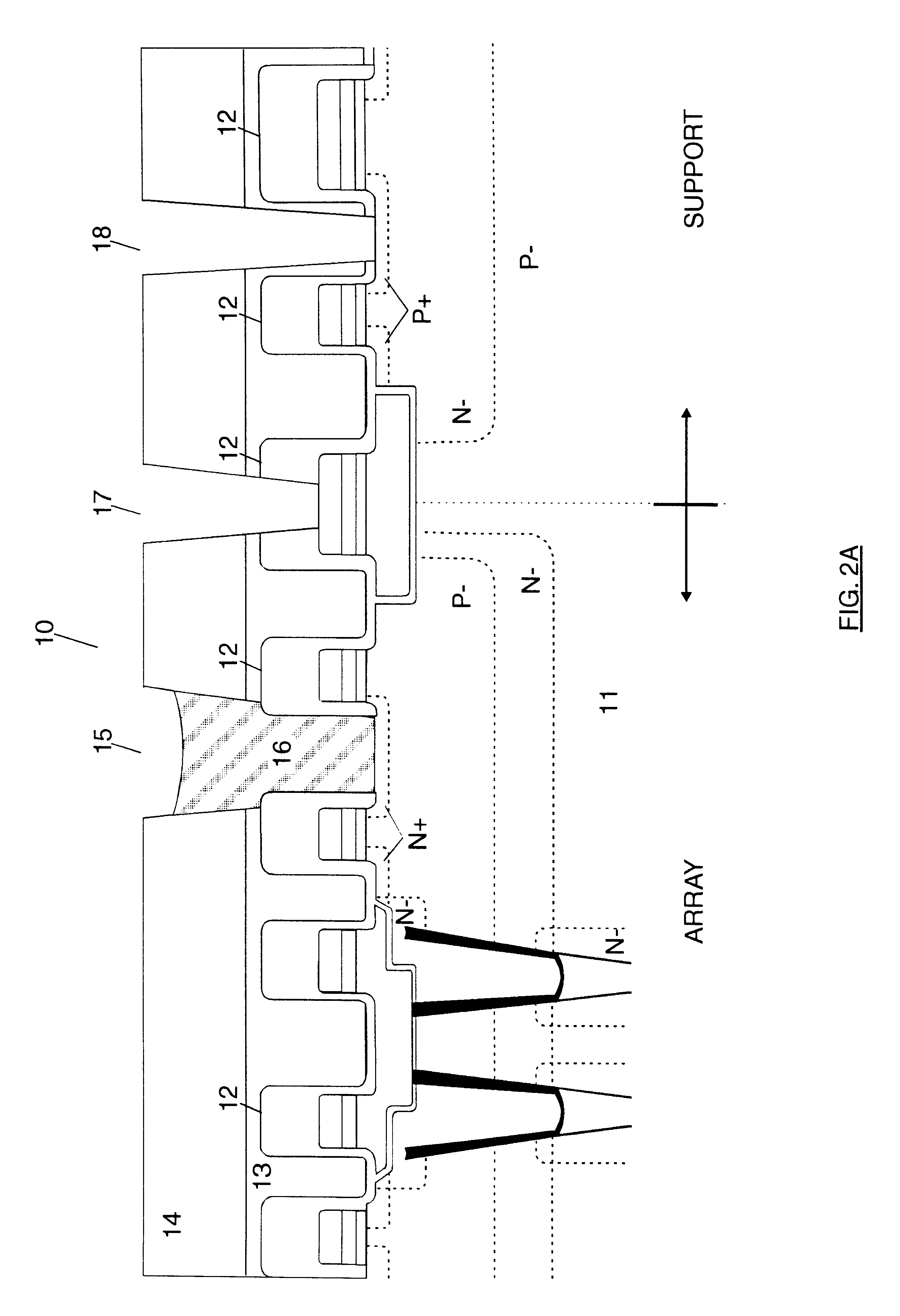
First of all, it has been experimentally demonstrated that to improve the process of etching the ARC layer 19 and the TEOS layer 14 to produce the desired M0 land recesses with an uniform result, the chemistry must not be selective, i.e., it must be able to etch ARC, TEOS and doped polysilicon materials at the same rate. Moreover this chemistry must not contain oxygen to avoid any degradation of the M0 land recess side walls. As a result, with such a chemistry, the step of etching the polysilicon stud 16 described by reference to FIG. 2A is no longer necessary and ...


PUM

PropertyMeasurementUnit
Temperatureaaaaaaaaaa

Abstract

The starting structure consists of a silicon substrate having diffused regions formed therein and gate conductor stacks formed thereupon that is passivated by a TEOS layer as standard. At a further stage of the wafer fabrication process, contact holes exposing some diffused regions and top of gate conductor stacks have been formed. At least one contact hole exposing a diffused region has been filled with doped polysilicon and the structure has been coated with a layer of an anti-reflective material (ARC) then, with a patterned mask to expose the ARC layer at the contact holes locations. The process improvement essentially consists in the use of a non selective chemistry which etches the doped polysilicon, the ARC and TEOS materials at substantially the same rate in a RIE etcher. A NF3/CHF3 gas mixture with a 23/77 ratio is adequate in that respect. The etch time duration is controlled first by an optical etch end-point detection system adapted to detect the signal transition at the TEOS layer exposure and then by an interferometric etch endpoint detection system to monitor the etched thickness to accurately stop when the selected depth for the M0 land recesses is reached. Finally, said recesses are filled with a metal (e.g. tungsten) as standard to produce the desired M0 metal lands.

Description

The present invention relates to the manufacture of semiconductor integrated circuits (ICs) and more particularly to a method of forming metal lands at the M0 level by plasma etching with a non selective chemistry.In the manufacture of semiconductor integrated circuits, and particularly in Dynamic Random Access Memory (DRAM) chips, a metal interconnect at the first level, referred to herein below as the M0 level, is extensively used to address memory cells of the chip. In essence, it is used to interconnect the source regions of all the Insulated Gate Field Effect Transistors (IGFETs) driven by the same Word Line (WL) and the gate conductors of all the IGFETs driven by a same Bit Line (BL) to their respective driving IGFET at the chip periphery. Each word line consists of a metal land which is formed at the M0 photolithography level.The essential steps of a conventional M0 metal lands formation process will be briefly described by reference to FIG. 1 and FIGS. 2A to 2E. After these ...

Claims


Application Information

Patent Timeline
IPC IPC(8): H01L21/02H01L21/70H01L21/768H01L21/311H01L21/3213H01L21/8242H01L27/108
CPCH01L21/31116H01L21/32137H01L27/10894H01L27/10882H01L21/76802H01L27/10829H10B12/37H10B12/48H10B12/09
Inventor MACCAGNAN, RENZO
Owner IBM CORP
Why Eureka
Try Eureka