Structure and method for forming a capacitor dielectric using yttrium barium copper oxide

a technology of yttrium barium copper oxide and capacitor dielectric material, which is applied in the direction of capacitors, basic electric elements, electrical appliances, etc., can solve the problems of reducing the surface area of capacitor dielectric materials formed using ono or on as capacitor dielectric materials, reducing the capacitance of capacitor dielectric materials, and material drawbacks,

Inactive Publication Date: 2001-10-09
TAIWAN SEMICON MFG CO LTD
View PDF6 Cites 19 Cited by
  • Summary
  • Abstract
  • Description
  • Claims
  • Application Information

AI Technical Summary

Benefits of technology

It is another object of the present invention to provide a method for forming a yttrium barium copper oxide film at low temperature having a high dielectric constant which can be easily patterned and provides good end point detection during etching.
It is yet another object of the present invention to provide an economical and manufacturable method for forming a high dielctric constant film for use as a capacitor dielectric layer.
The present invention provides considerable improvement over the prior art. A sputter deposited and annealed yttrium barium copper oxide layer with the oxygen content controlled at at the desired level can provide a dielectric constant of between about 70 and 100, which is about 10 times higher than ONO. A capacitor dielectric layer using this high dielectric constant material allows higher packing density because comparable capacitance can be acheived with less surface area.
By using a sputter process to deposit the high dielectric constant yttrium barium copper oxide layer, it can be deposited at lower temperatures than other capacitor dielectric materials known in the art. It can also be formed at lower temperatures than other "YBCO" processes described in the prior art. This lower processing temperature is particularly advantagous in DRAM fabrication. The sputter deposition and anneal steps of the present invention provide good control of thickness and oxygen content, thereby providing good control of the dielectric constant. Also, yttrium barium copper oxide is easy to pattern and its black color makes end point detection easy.

Problems solved by technology

However, as device dimensions continue to shrink, capacitors formed using ONO or ON as the capacitor dielectric material are not able to provide the necessary capacitance with the reduced surface area.
Each of these materials suffer drawbacks for use as a capacitor dielectric material for mass production of silicon-based intergrated circuits.
While these leakage currents can be reduced using a high temperature anneal, high temperature anneals are detrimental to DRAM devices.
Also, BST and PZT are difficult to deposit as thin films.

Method used


Image

  • Structure and method for forming a capacitor dielectric using yttrium barium copper oxide
  • Structure and method for forming a capacitor dielectric using yttrium barium copper oxide
  • Structure and method for forming a capacitor dielectric using yttrium barium copper oxide

Examples


Embodiment Construction

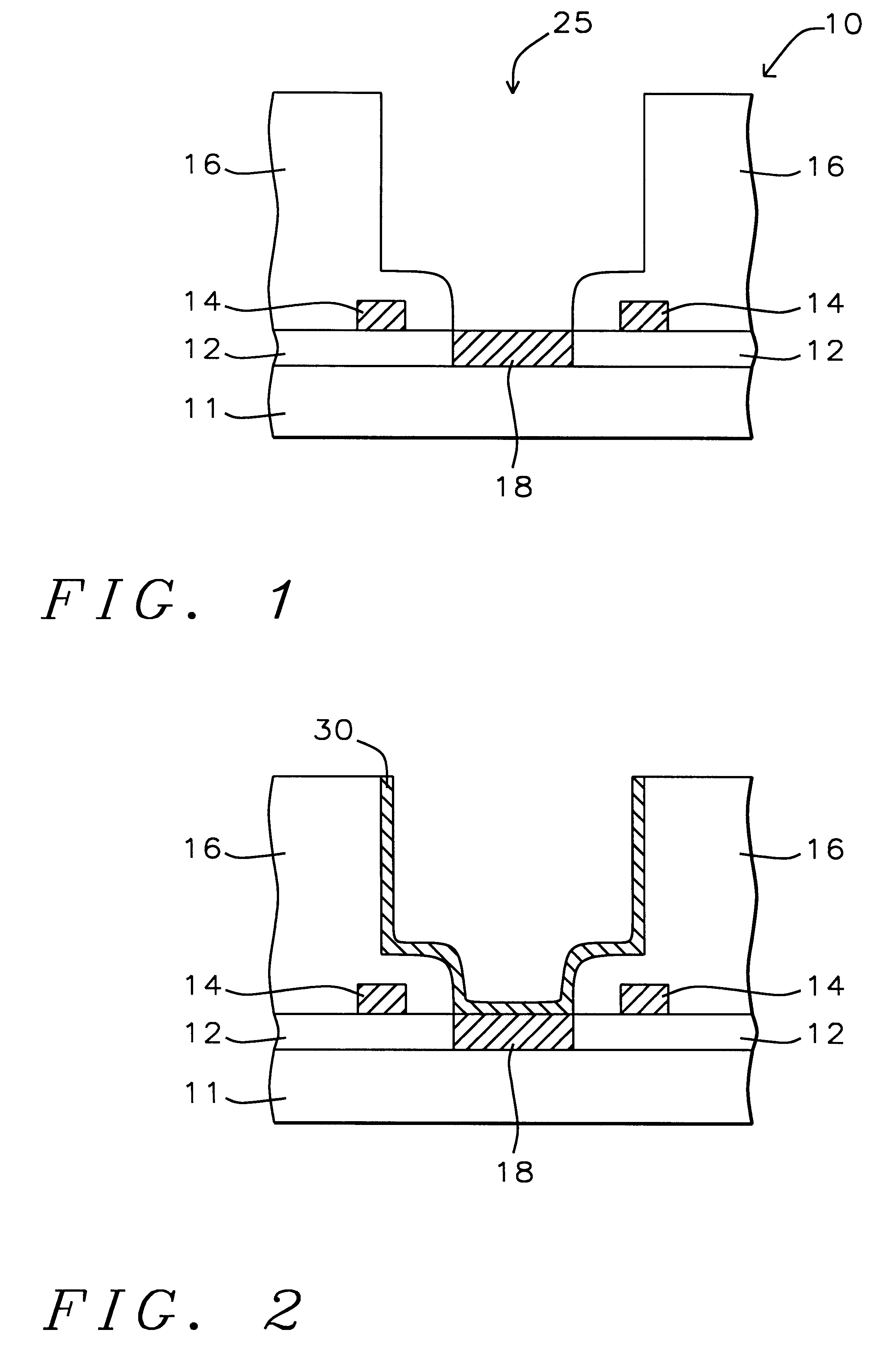
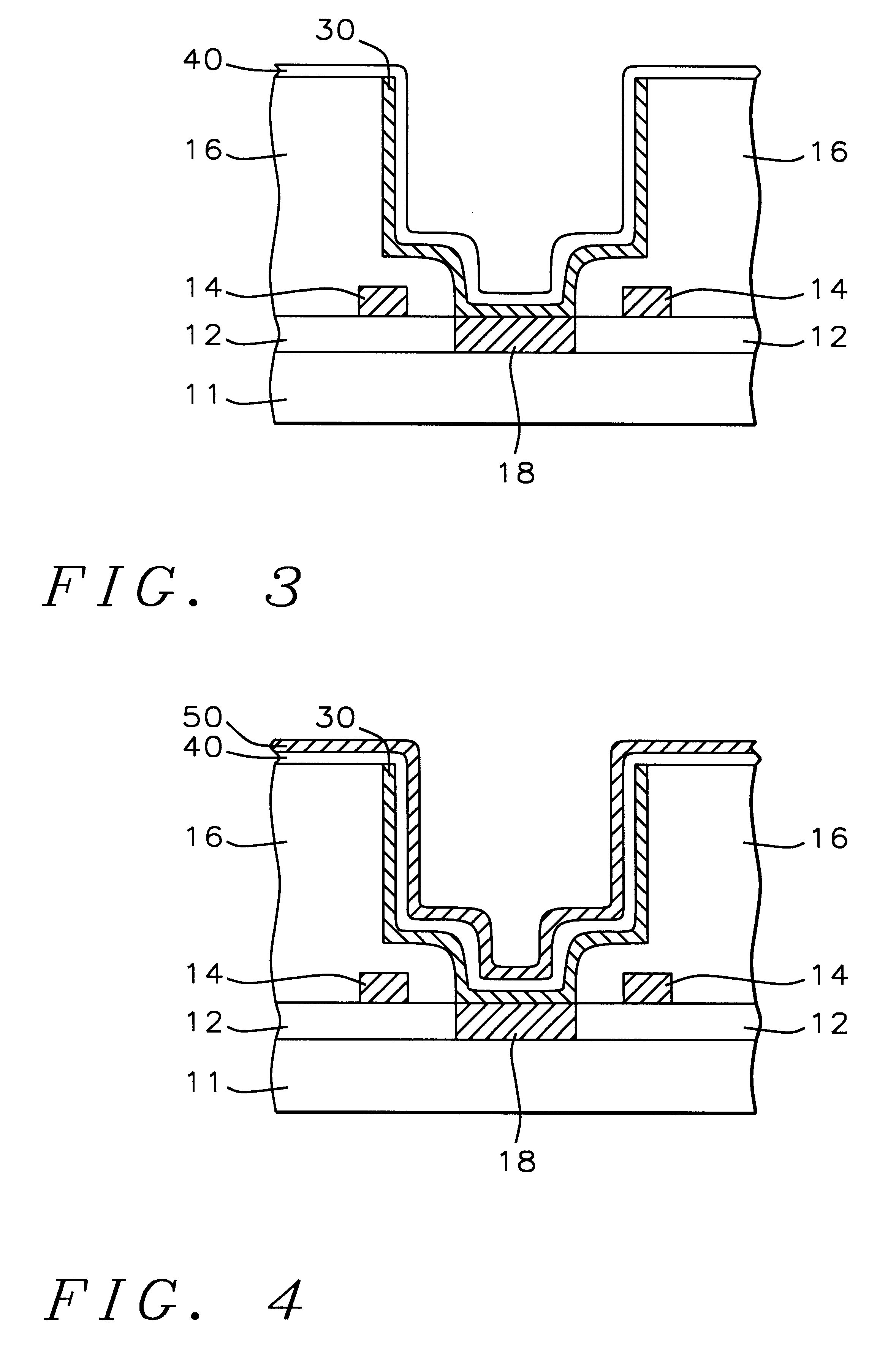
A preferred embodiment of the present invention will be described in detail with reference to the accompanying drawings. In this preferred embodiment, a method and structure for a capacitor is described, using a sputter deposited and vacuum annealed yttrium barium copper oxide layer as a capacitor dielectric layer.

Referring to FIG. 1, the process begins by providing a semiconductor structure (10) such as for a DRAM. Semiconductor structure is to be understood to include a substrate such as a silicon wafer, and to possibly include one more conductive layers and / or dielectric layers overlying the substrate. Semiconductor structure is understood to possibly further include one or more devices formed in the substrate and / or overlying layers. The semiconductor structure (10) illustrated in FIG. 1 comprises a substrate (11) with an overlying first dielectric layer (12) having bit lines (14) on the first dielectric layer (12) and a conductive plug (18) formed in the first dielectric layer ...


PUM

PropertyMeasurementUnit
thicknessaaaaaaaaaa
thicknessaaaaaaaaaa
thicknessaaaaaaaaaa

Abstract

A method and structure for forming a capacitor in a semiconductor device using a high dielectric constant, yttrium barium copper oxide layer as the capacitor dielectric layer. The process begins by providing a semiconductor structure having a conductive plug therein and having an opening, with sidewalls, over the conductive plug. The opening is shaped to accomodate a capacitor structure as is known in the art. A first conductive layer is formed on the conductive plug and on the sidewalls of the opening. A yttrium barium copper oxide layer is deposited on the first conductive layer using a sputtering process with a YBa2Cu3O7 target. The yttrium barium copper oxide layer can be annealed to control the oxygen content. For example, YBa2Cu3O6+X can be controlled at between X=0.2 and X=0.5. A second conductive layer is formed on the yttrium barium copper oxide layer, thereby forming a capacitor comprising the first conductive layer, the yttrium barium copper oxide layer, and the second conductive layer.

Description

BACKGROUND OF INVENTION1) Field of the InventionThis invention relates generally to fabrication of a semiconductor device and more particularly to a structure and method for forming a capacitor on a semiconductor structure by depositing a yttrium barium copper oxide layer over a first plate electrode layer at room temperature using a sputtering process.2) Description of the Prior ArtCurrently, oxide / nitride / oxide (ONO) or oxide / nitride (ON) stacks are primarily used as capacitor dielectric layers in DRAM fabrication. However, as device dimensions continue to shrink, capacitors formed using ONO or ON as the capacitor dielectric material are not able to provide the necessary capacitance with the reduced surface area.New high dielectric constant materials have been developed to provide increased capacitance for a given surface area. Among these newly developed materials are Ta2O5, BST, and PZT. Each of these materials suffer drawbacks for use as a capacitor dielectric material for mass...

Claims


Application Information

Patent Timeline
Patent Type & Authority Patents(United States)
IPC IPC(8): H01L21/02
CPCH01L28/55
Inventor SHAN, PAO-CHUAN
Owner TAIWAN SEMICON MFG CO LTD
Why Eureka
Try Eureka