Growth method for silicon nanowires and nanoparticle chains from silicon monoxide

a growth method and nanoparticle technology, applied in the direction of crystal growth process, polycrystalline material growth, chemically reactive gas, etc., can solve the problems of limited number of nanowire strands, low yield of production, and tedious methods, so as to reduce system energy, reduce surface energy, and enhance one-dimensional growth

Inactive Publication Date: 2001-11-06
HONG KONG CITY UNIV OF
View PDF5 Cites 169 Cited by
  • Summary
  • Abstract
  • Description
  • Claims
  • Application Information

AI Technical Summary

Benefits of technology

Applicants further theorize that the growth process of silicon nanowire involves the following factors (see FIG. 6(b)). The relatively thick Si.sub.x O on the tips of nanowire acts as a catalyst. The SiO.sub.2 component in the shell, which is formed during decomposition of Si.sub.x O for nanowire growth, retards the lateral growth of nanowires. Defects, such as stacking faults in the nucleus tips, enhance the one-dimensional growth. The {111} surface, which has the lowest surface energy among the surfaces in silicon, plays an important role during nanowire growth. Since surface energy is more important when the crystal size is largely reduced down to nanometer scale, the appearance of {111} surfaces of the silicon crystals parallel to the axes of the nanowires reduces the system energy. These factors collectively determine the growth direction of silicon nanowires to be <112>direction. According to Applicant's investigations, nucleation and growth occur at all times during evaporation since the SiO vapor phase is continually generated. Nuclei may form on the nanowire tips with different crystalline orientations during growth. These unfavorable nuclei cannot grow fast along the nanowire and would cause a change of growth direction or re-nucleation. Such re-nucleation processes resulted in the formation of the nanoparticle chains (see FIGS. 5(a) and (b)) which co-existed with the nanowires.

Problems solved by technology

These methods are tedious and normally produce only a limited number of strands of nanowires.
The drawbacks of the VLS technique in producing nanowires are (1) contamination by the metal catalyst and (2) the extremely low yield of production, Therefore, one of the challenging issues in the field of silicon nanostructures has been the synthesis of high-quality, high purity silicon nanowires in large quantities.

Method used


Image

  • Growth method for silicon nanowires and nanoparticle chains from silicon monoxide
  • Growth method for silicon nanowires and nanoparticle chains from silicon monoxide

Examples


example 2

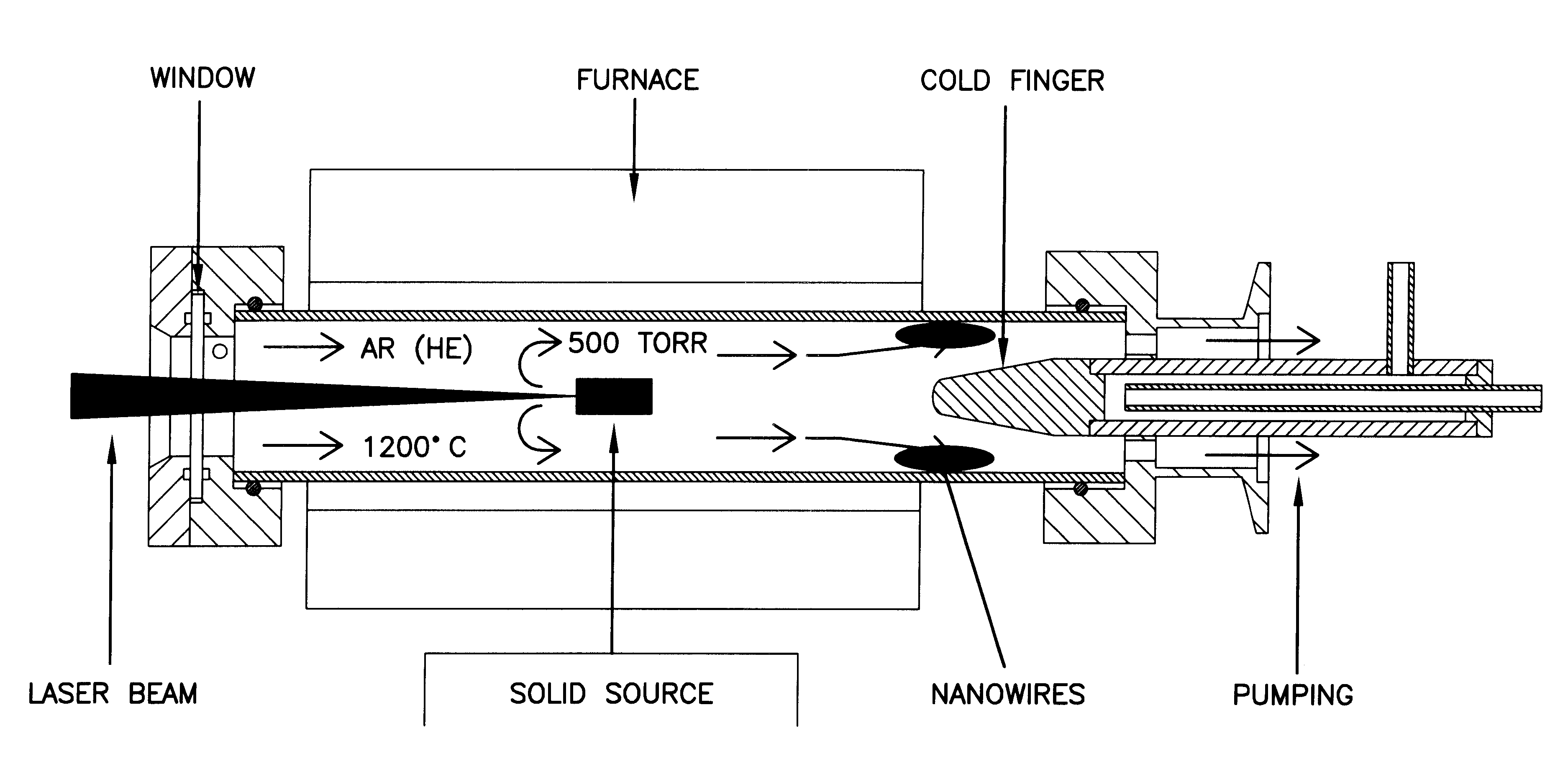
In this example, the same apparatus shown in FIG. 1 is used. The solid source is a mixture of SiO.sub.2 and Si (or Ge) in equal-molar ratio. The temperature around the solid source is about 1200.degree. C. Silicon nanowires grow at about 950.degree. C. The growth rate is slower than that in example 1. The growth time is about 10 hours. In this growth process, silicon monoxide vapor phase was generated by the following reaction in the solid source.

Si+SiO.sub.2.fwdarw.2SiO

and

Ge+SiO.sub.2.fwdarw.SiO+GeO

The temperature for this reaction is at least 1100.degree. C. The morphology and microstructure of silicon nanowires and nanoparticle chains are similar to that grown in example 1.

example 3

In this example, the apparatus, solid source and experimental conditions (temperature, pressure, etc.) are the same as that used in example 2. An Excimer laser (wave length=248 nm, frequency=10 Hz) is used to assist the generation of silicon monoxide vapor phase. The growth rate is increased and the growth time is shortened to 1 hour.


PUM

PropertyMeasurementUnit
pressureaaaaaaaaaa
temperatureaaaaaaaaaa

Abstract

Silicon nanowires and silicon nanoparticle chains are formed by the activation of silicon monoxide in the vapor phase. The silicon monoxide source may be solid or gaseous, and the activation may be by thermal excitation, laser ablation, plasma or magnetron sputtering. The present invention produces large amounts of silicon nanowires without requiring the use of any catalysts that may cause contamination.

Description

This invention relates to a method of using silicon monoxide or suboxide for the growth of high-purity silicon nanowires and silicon nanoparticle chains in bulk-quantity.Materials engineering at the nanometer scale can provide smaller devices than those currently available. In particular, research on semiconductor nanostructures with size-dependent optical and electronic properties, such as quantum-dots, one-dimensional quantum wire transistors and light emitting devices with extremely low power consumption is motivated by potential applications. Silicon is a material of great interest for nanostructures because of its important role in the field of microelectronics.Since the 1960's, silicon whiskers grown by the vapor-liquid-solid (VLS) reaction have been extensively studied. After the VLS technique, many efforts have been made to further improve the synthesis of silicon nanowires by employing different techniques, such as photolithography technique combined with etching and scanni...

Claims


Application Information

Patent Timeline
Patent Type & Authority Patents(United States)
IPC IPC(8): C30B23/00
CPCC30B23/00C30B29/605C30B29/06Y10S977/891Y10S438/962
Inventor LEE, SHUIT-TONGWANG, NINGLEE, CHUN-SINGBELLO, IGOR
Owner HONG KONG CITY UNIV OF
Why Eureka
Try Eureka