Planarization compositions and methods for removing interlayer dielectric films

a technology of dielectric films and compositions, applied in the direction of polishing compositions, other chemical processes, manufacturing tools, etc., can solve the problems of unsuitable manufacture surface roughness, insufficient planarity of the resultant gap-filled surface, and large number of scratches on the planar surface. achieve the effect of improving the quality of planarization of dielectric films

Inactive Publication Date: 2001-11-27
ADVANCED TECH MATERIALS INC
View PDF87 Cites 112 Cited by
  • Summary
  • Abstract
  • Description
  • Claims
  • Application Information

AI Technical Summary

Benefits of technology

To demonstrate the effectiveness of the invention, a planarization composition comprising an ethyl silicate slurry was used, having the following physical and chemical characteristics:
The above composition was used to polish semiconductor substrates, BPTEOS (12,000 .ANG. thick), and thermal oxide (6,000 .ANG. thick). The polishing pad was a Rodel model IC1000-A1 CMP device. The example comprises positioning the planarizing composition set forth above between a pad and the surface coating and rubbing the pad against the surface coating according to the following planarizing parameters:
The amounts of material removed for BPTEOS and thermal oxide were 3,910 .ANG. and 1,018 .ANG., respectively. The polishing rates for the above thin films were 4,887 .ANG. and 1,272 .ANG. per minute, respectively. Unexpectedly and surprisingly, the within wafer non-uniformities for BPTEOS and thermal oxide were less than 3.5% and surface roughness for both BPTEOS and thermal oxide were less than 6.0 .ANG.. In contrast with these results, polishing using prior art slurries, resulted in root mean square su

Problems solved by technology

However, after this dielectric gap-fill process, the planarity of the resultant gap-filled surface is not planar enough to be used as an imaging plane upon which the next pattern of circuitry is defined by photolithographic techniques.
This is due to the non-planar scratched and rough regions being "out-of-focus" relative to the planar unscratched and smooth regions.
The result, however, is a planarized surface that has a substantial number of scratches and a surface roughness that is not suitable for the manufacture of integrated circuits which utilize sub 0.3 5-micron geometries.
Further, in addition to the polishing and planarizing rates for this method being too low to be production-worthy, this type of thinning, polishing and planarizing slurry is considered too dirty having high levels of potential yield-limiting metal ion impurities incorporated in the liquid carrier and the silica slurry abrasive.
Further, the resulting colloidal silica had unacceptably high ammonia and alcohol contents that prohibited them from being used broadly in silica wafer polishing and frm being used for interlayer dielectric and shallow trench isolation CMP.
A very real problem exists with respect to polishing materials such as insulating dielectric films without scratches and sufficiently low enough surface roughness and post-planarization surface and dielectric film cleanliness.
Insulating thin films are deposited within the channels which fills the channels but still leaves the dielectric thin film surface not planar enough.
Today's state of the art planarization process, although at one time was sufficient enough to fully planarize the dielectric surface, is no longer sufficient.
Scratches (macro-scratches) and haze (micro-scratches and light-point defects), which were once not considered yield-limiting defects, are considered yield-limiting defects today and today's benign scratches and haze most likely will become more substantial yield-limiting factors with tomorrow's more advanced, higher performance, integrated circuits.
Today's abrasives used for dielectric planarization are almost exclusively fumed silica whose particle size distribution and shape cause undesirable surface scratches and haze.
Sodium and potassium are considered the most dangerous yield-limiting contaminants to integrated circuits during their manufacture and therefore the use of precipitated silicas have not gained industry-wide acceptance.
Further, there are other high levels of yield-limiting impurities in precipitated silica slurries such as alkaline ea

Method used


Image

  • Planarization compositions and methods for removing interlayer dielectric films
  • Planarization compositions and methods for removing interlayer dielectric films
  • Planarization compositions and methods for removing interlayer dielectric films

Examples


example 1

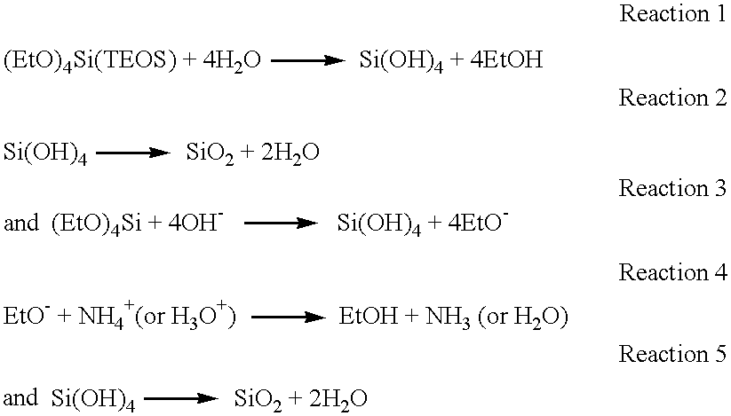
Method 1 for Manufacturing Ethyl Silicate Slurry

1. Materials

Solution A: 73 milliliters (ml) 28% ammonium hydroxide (NH.sub.4 OH; concentration: 2.07 mol / l) 41 ml water (H.sub.2 O; concentration: 26.94 mol / 1) 8 ml ethyl alcohol (ETOH; concentration: 0.16 mol / l)

Solution B: 46 ml TEOS; (final concentration: 1.92 mol / l).

2. Synthesis of Primary Particles

a. Warm a beaker to 33.degree. C. to 37.degree. C.

b. Add solutions A and B dropwise over 15 minutes, with constant stirring at 280 rpm into beaker with the flow rate of A twice the flow rate of B.

c. remove from heat, stir, cool to 21.5.degree. C. over 15 min.

3. Growth of Final Particles

a. Warm solution to 35.degree.-37.degree. C. while adding dropwise with stirring: 250 ml TEOS and 394 ml H.sub.2 O.

b. Stir for 1.0 hours in a closed vessel.

c. Add 30 mnl TEOS dropwise every 30 minutes for a total of 3 additions.

d. Particle size: 160-180 nm.

4. Final Slurry Composition (weight percent of total)

a. 12.95% silica (SiO.sub.2)

b. 2.0% NH.sub.3

c. 40...

example 2

Method 2 for Manufacturing Ethyl Silicate Slurry

1. Materials

a. Solution A: 123 ml of 28% NH.sub.4 OH; (concentration: 6.96 mol / l) 60 ml H.sub.2 O; (concentration: 19.78 mol / l) 10 ml ETOH; (concentration: 0.31 mol / l)

b. SolutionB: 24 ml 28% NH.sub.4 OH and 133 ml H.sub.2 O.

2. Synthesis of Primary Particles

a. Pre-warm beaker to 33.degree. C. to 37.degree. C.

b. Add Solution A to beaker dropwise over 30 minutes along with 77 ml TEOS with constant stirring at 280 rpm and flow rate of Solution A being twice the flow rate of TEOS (final TEOS concentration, 1.59 mol / l).

3. Growth of Final Particles

a. To the solution containing primary particles, add Solution B and 115 ml TEOS, both dropwise over 30 minutes, with constant stirring and with the flow rate of Solution B being twice that of the TEOS. After 2 / 3 of the TEOS has been added, the heat is turned off.

b. Stir for 1 hour more in a closed vessel.

example 3

Method 3 for Manufacturing Ethyl Silicate Slurry for CMP

1. Materials

a. Solution A: 147 ml NH.sub.4 OH, (concentration: 6.71 mol / l) 72 ml H.sub.2 O, (concentration: 19.38 mol / l) ml ETOH, (concentration: 0.36 mol / l)

b. SolutionB: 124 mlH.sub.2 O.

2. Synthesis of Primary Particles

a. Pre-warm beaker to 33.degree. C. to 37.degree. C.

b. Add Solution A and 92 mnl TEOS over 15 minutes, stir at 280 rpm with the flow rate of Solution A being twice the flow rate of the TEOS solution. (final TEOS concentration: 1.65 mol / l)

c. Let cool while stirring, over 15 minutes to 21.5.degree. C.

d. Particle size: 160-180 nm.

3. Growth of Final Particles

a. Warm the solution containing primary particles to 33.degree. C. to 37.degree.. Cover 30 minutes while adding Solution B and 115 ml TEOS, with the flow rate of Solution B being twice the flow rate of the TEOS. Reduce the heat after 1 / 3 of the TEOS has been added.

b. Stir in a closed vessel for 1 hour.

c. Particle size: 160-180 nm.


PUM


Abstract

A planarization composition is set forth for chemical mechanical planarization of dielectric layers for semiconductor manufacture. The composition comprises spherical silica particles having an average diameter of from 30 nm to about 400 nm, and a narrow range of particle sizes, wherein about 90% of the particles is within 20% of the average particle diameter. The composition includes a liquid carrier comprising up to about 9% alcohol and an amine hydroxide in the amount of about 0.2 to about 9% by weight. The pH of the composition is in the range of about 9 to about 11.5, and the remainder of the solution is water. The composition has low amounts of metal ions, and the composition is used for thinning, polishing and planarizing interlayer dielectric thin films, shallow trench isolation structures, and isolation of gate structures. The invention also comprises methods for using the planarization composition in the manufacture of semiconductor devices.

Description

I. Technical FieldThe present invention relates to a planarization composition which is particularly useful for thinning, polishing and planarizing integrated circuitry deposited on semiconductor wafers which have an inter-layer dielectric material deposited on their surfaces to form insulating dielectric films. The thinning, polishing and planarizing serves to remove a portion of the dielectric film so as to flatten and smoothen the deposited dielectric surface, and further to remove excess deposited dielectric material during the formation of shallow trench isolation structures. The invention also relates to a thinning, polishing and planarizing apparatus and method for carrying out the thinning, polishing and planarizing process to flatten and smoothen the dielectric film and to remove excess deposited dielectric material during the formation of shallow trench isolation structures.II. Discussion of Related ArtIn semiconductor processing, it is common to deposit a thin film of an ...

Claims


Application Information

Patent Timeline
IPC IPC(8): C09K3/14C09G1/00C09G1/02H01L21/02H01L21/3105
CPCC09G1/02C09K3/1463H01L21/31053
Inventor BREWER, RICHARDGREBINSKI, THOMAS J.CURRIE, JAMES E.JONES, MICHAELMULLEE, WILLIAMNGUYEN, ANN
Owner ADVANCED TECH MATERIALS INC
Why Eureka
Try Eureka