Method for repairing pattern defect, photo mask using the method, and semiconductor device manufacturing method employing the photo mask

a pattern defect and manufacturing method technology, applied in the field of pattern defect repair, can solve the problems of high accuracy, troublesome task, excessive etching around the perimeter of microscopic defect that needs to be eliminated,

Inactive Publication Date: 2002-01-01
KK TOSHIBA
View PDF9 Cites 80 Cited by
  • Summary
  • Abstract
  • Description
  • Claims
  • Application Information

AI Technical Summary

Problems solved by technology

As the feature size of such a photo mask pattern becomes significantly finer and finer, its repairing process at a high accuracy will be very difficult with a laser beam scanning precisely along the edge of the line pattern.
Also, since the focusing of the laser beam is limited, the pattern defect repairing at higher accuracy, which may require a laser beam diameter finer than 0.5 .mu.m, will thus be a troublesome task.
Moreover, the diffused FIB and the beam expansion of the FIB may result in excessive etching around the perimeter of the microscopic defect that needs to be eliminated.
However, it was found that, in finer masks used for exposure by Deep UV (DUV) rays or further shorter wavelength rays, the chromium film repaired by the gas assisted FIB etching process still has noticeable damages to the mask substrate, attributable to the gallium stains or the riverbed.
The gas assisted FIB etching process may rarely be effective for repairing microscopic defect on a phase shift mask when it is made of a silicon based material such as molybdenum silicide (MoSi, or MoSi.sub.x) and used as the film material for producing the light-shielding pattern or the phase shifter pattern.
Damage to the mask substrate may result in deterioration of the transparency of the mask substrate.

Method used


Image

  • Method for repairing pattern defect, photo mask using the method, and semiconductor device manufacturing method employing the photo mask
  • Method for repairing pattern defect, photo mask using the method, and semiconductor device manufacturing method employing the photo mask
  • Method for repairing pattern defect, photo mask using the method, and semiconductor device manufacturing method employing the photo mask

Examples


first embodiment

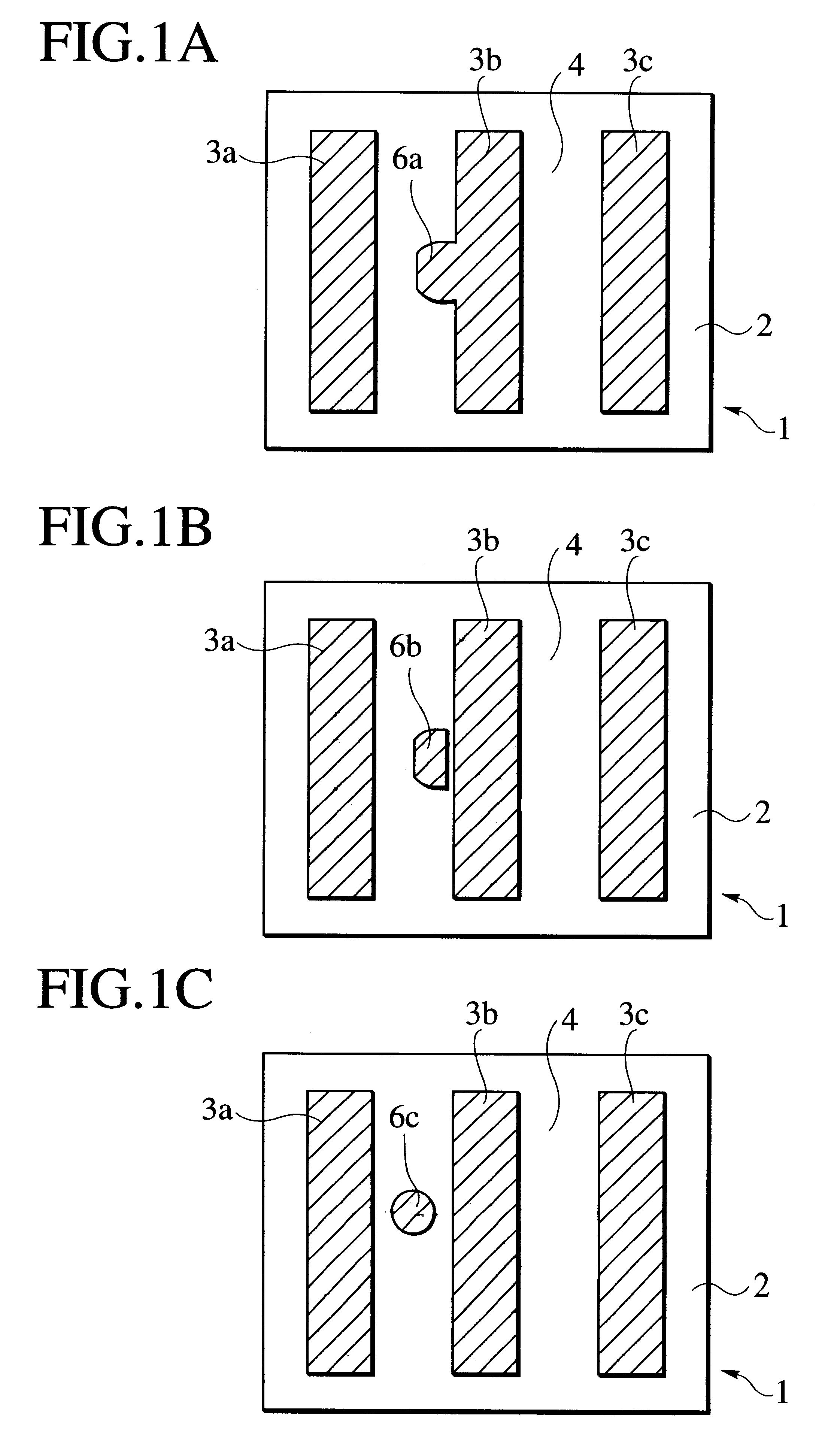
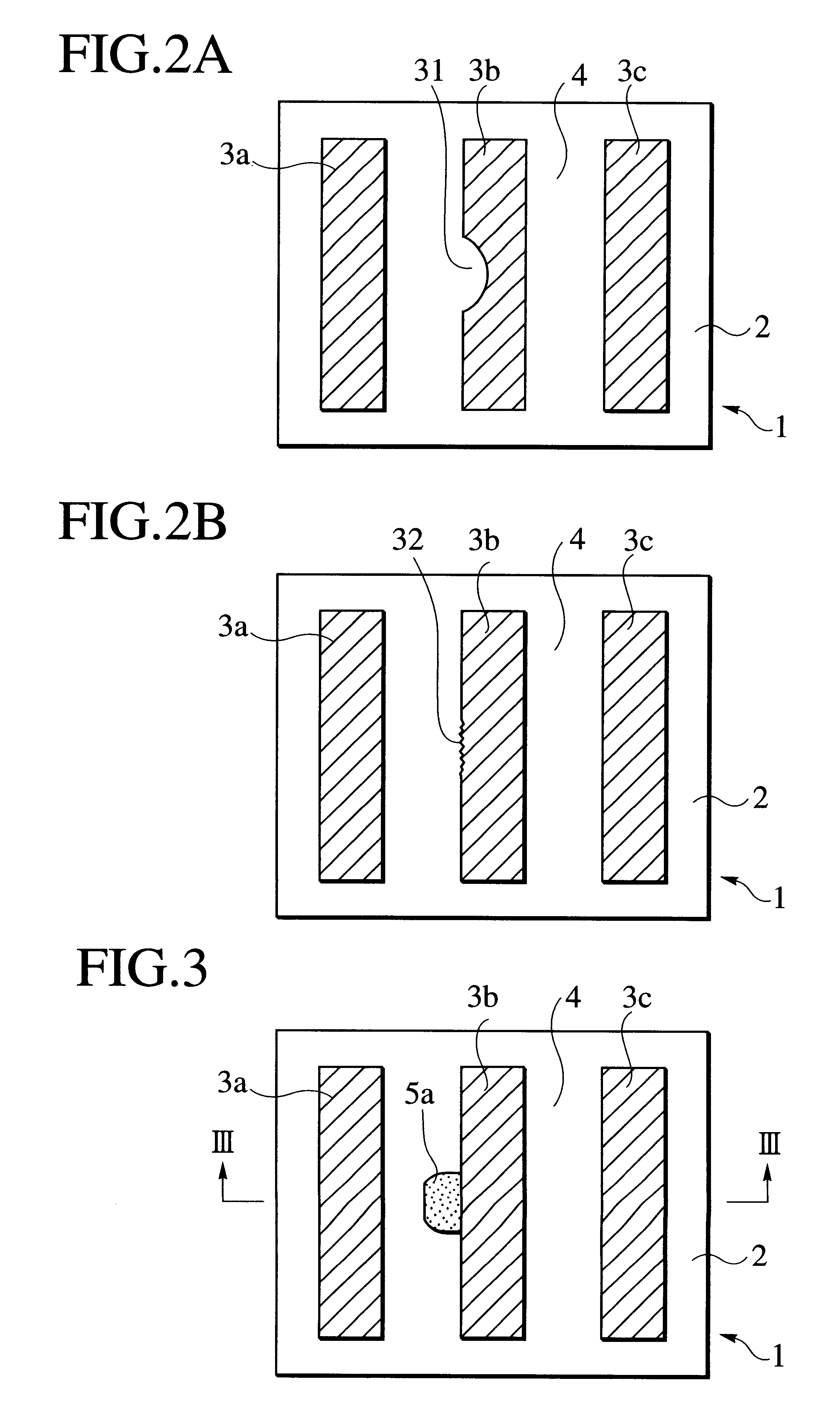
The mask defect repairing method according to the present invention will now be described. Here, an excessive portion of the pattern film material, or the microscopic defect 6a generated on the chromium mask 1, will be eliminated. The chromium mask 1 has the chromium light-shielding lines 3a, 3b and 3c delineated on the quartz substrate 2 as shown in FIG. 5.

(a) First, as shown in FIG. 6A, the microscopic defect 6a is sputtered by a FIB 7 with an assistant gas 8 for chromium film etching. The assistant gas 8 is sprayed over the mask surface. In other words, a gas assisted FIB etching process carries out the etching. As described in the section of BACKGROUND OF THE INVENTION, riverbeds may possibly be created around the microscopic defect 6a by the effect of a diffused FIB or beam expansion of the FIB. For compensation, the exposure area about the microscopic defect 6a to the ion beam, directed towards the transparent quartz substrate 2, is inwardly narrowed by 0.3 nm to 200 nm from t...

second embodiment

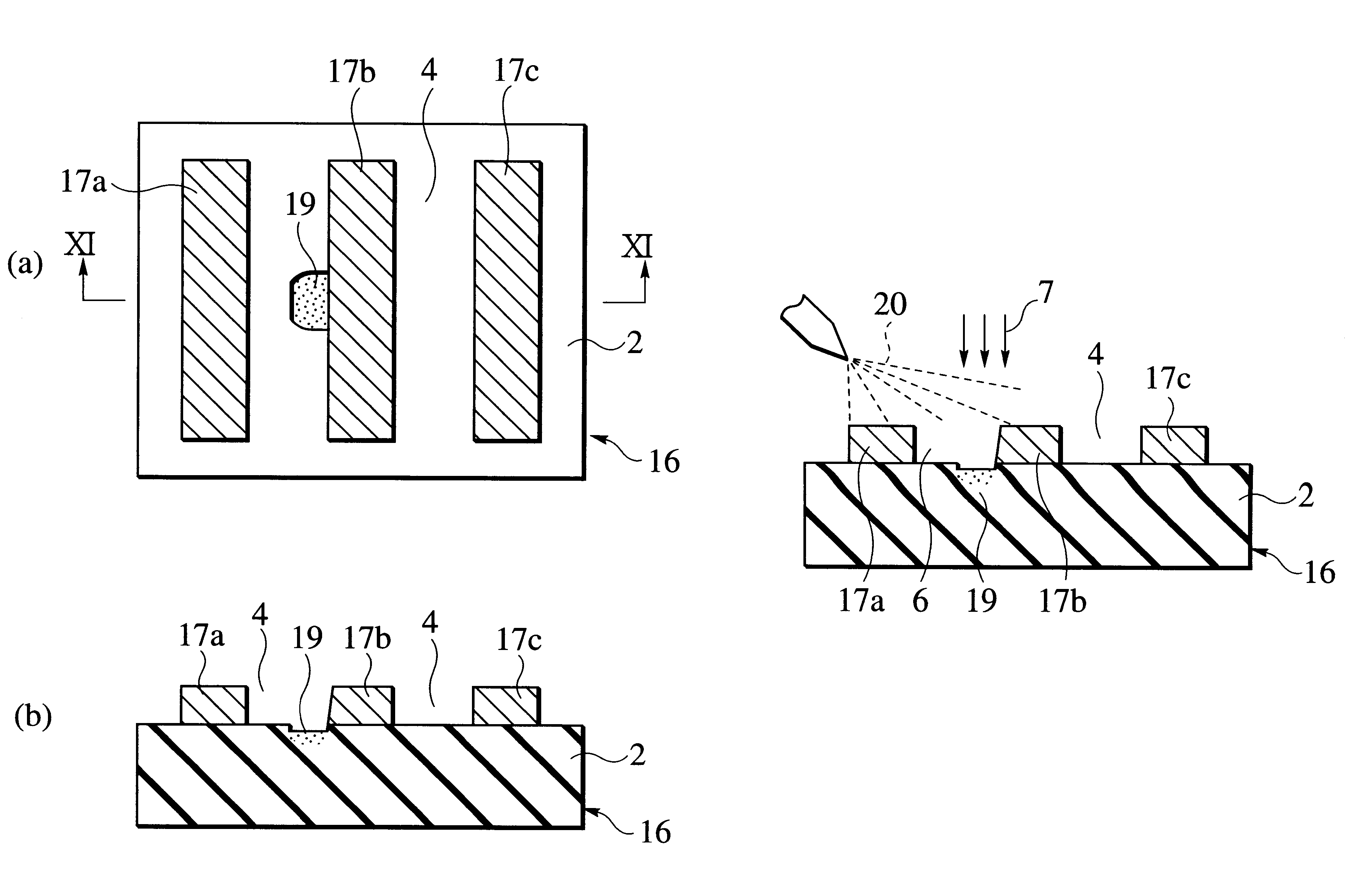
A second embodiment of the present invention will be described in the form of a mask defect repairing method of eliminating a microscopic defect 6a generated on a phase shifter 17b made of an oxide nitride of molybdenum silicide (MoSiO.sub.x N.sub.y) as a pattern film material delineated on a quartz substrate 2. Instead of MoSiO.sub.x N.sub.y, an oxide of molybdenum silicide (MoSiO.sub.x), or composite film of MoSiO.sub.x N.sub.y / MoSi and MoSiO.sub.x / MoSi can also be employed for the phase shifter 17b. The molybdenum silicide phase shifter 17b is referred to as "the phase shifter 17b" hereinafter. And a molybdenum silicide phase shifter pattern may be called as "a phase shifter pattern".

A phase shift mask 16 shown in FIG. 9 comprises the line pattern of phase shifter 17b made of the oxide nitride of molybdenum silicide and another line patterns 17a and 17c delineated on the transparent quartz substrate 2. The line patterns 17a and 17c can be made of the oxide nitride of molybdenum...

third embodiment

Third embodiment of the present invention pertains a method of mask repairing a microscopic defect 6a generated on a phase shift mask 22. The phase shift mask 22 of the third embodiment is composed of chromium / molybdenum silicide patterns 23a, 23b and 23c formed on a transparent quartz substrate 2. Each of the chromium / molybdenum silicide patterns 23a, 23b and 23c consists of the corresponding phase shift pattern 17a, 17b or 17c made of an oxide nitride of molybdenum silicide and a chromium film 24a, 24b or 24c provided on the phase shift pattern 17a, 17b or 17c, respectively. That is, the chromium films 24a, 24b and 24c are multi-layers, or composite films, comprising chromium layers and chromium oxide layers developed on the chromium layers, respectively.

In the boundary between shots, the lights penetrating the phase shift films overlap, when the mask pattern is projected on the wafer, so that the resist film formed on the wafer is unintentionally exposed. It is necessary to shiel...


PUM

PropertyMeasurementUnit
distanceaaaaaaaaaa
thicknessaaaaaaaaaa
diameteraaaaaaaaaa

Abstract

A new method for repairing pattern defect on a photo mask is provided. The method includes the steps of: (a) determining the irradiation area of the focused ion beam (FIB) directed towards a defect, by narrowing the irradiation area by a predetermined distance inwardly from the edge of the defect; (b) focusing the FIB onto its irradiation area to remove a part of the pattern film material of the defect from its top surface and thus leave a thin layer on a mask substrate; and (c) removing the thin layer by using a laser beam. The defect may be an isolated pattern or a pattern extended continuously from an edge of the normal pattern. Further, the photo mask repaired by the method, and a manufacturing method of semiconductor devices employing the repaired photo mask are proposed. The photo mask may include a phase shift mask.

Description

1. Field of the InventionThe present invention relates to a method for repairing a pattern defect on a photo mask, the photo mask repaired by the repairing method, and a manufacturing method of semiconductor devices employing the repaired photo mask. The photo mask may include a phase shift mask.2. Description of the Related ArtIn the manufacturing method of the semiconductor devices such as large scale integrations (LSls), very large scale integrations (VLSIs), ultra large scale integrations (ULSIs), and giga scale integrations (GSIs), a set of photo masks or reticles is required for photolithography steps. Each of the photo masks is composed of predetermined patterns made of a light-shielding layer or phase shift layer arranged on a transparent mask substrate, such as a quartz substrate. During the fabrication process of the photo masks, miscellaneous microscopic defects 6a, 6b, 6c may be created on the mask substrate as shown in FIGS. 1A, 1B and 1C, for example. In each of FIGS. ...

Claims


Application Information

Patent Timeline
Patent Type & Authority Patents(United States)
IPC IPC(8): G03F1/00H01J37/305B23K26/00G03F1/26G03F1/68G03F1/72G03F1/74G03F7/20H01L21/027
CPCG03F1/74H01J37/3056H01J2237/31742
Inventor ASANO, MITSUYOKANAMITSU, SHINGO
Owner KK TOSHIBA
Why Eureka
Try Eureka