Chemical vapor deposition process for depositing titanium nitride films from an organometallic compound

a technology of titanium nitride and chemical vapor deposition, which is applied in the direction of chemical vapor deposition coating, coating, plasma technique, etc., can solve the problems of high temperature involved in the process, poor step coverage of the film, and incompatibility with the conventional manufacturing process of integrated circuits

Inactive Publication Date: 2002-01-15
MICRON TECH INC
View PDF2 Cites 30 Cited by
  • Summary
  • Abstract
  • Description
  • Claims
  • Application Information

AI Technical Summary

Problems solved by technology

Each of the processes enumerated above has its associated problems.
Both reactive sputtering and nitrogen ambient annealing of deposited titanium result in films having poor step coverage, which are not useable in submicron processes.
The high temperatures involved in this process are incompatible with conventional integrated circuit manufacturing processes.
The low-temperature APCVD, on the other hand, though performed within a temperature range of 100-400.degree. C. that is compatible with conventional integrated circuit manufacturing processes, is problematic because the precursor compounds (ammonia and Ti(NR.sub.2).sub.4) react spontaneously in the gas phase.
In spite of special delivery systems, the highly spontaneous reaction makes full wafer coverage difficult to achieve.
Even when achieved, the deposited films tend to lack uniform conformality, are generally characterized by poor step coverage, and tend to deposit on every surface within the reaction chamber, leading to particle problems.
A problem with the LPCVD process is that the deposited TiN films are high in carbon content even if the precursor is limited to tetrakis-dialkylamido- titanium, the compound of the group which contains the fewest carbon atoms.
Although it is possible to reduce the carbon content of the films by annealing them in ammonia and nitrogen gases, the films attain neither the purity nor the conductivity of sputtered films.

Method used


Image

  • Chemical vapor deposition process for depositing titanium nitride films from an organometallic compound
  • Chemical vapor deposition process for depositing titanium nitride films from an organometallic compound
  • Chemical vapor deposition process for depositing titanium nitride films from an organometallic compound

Examples


first embodiment

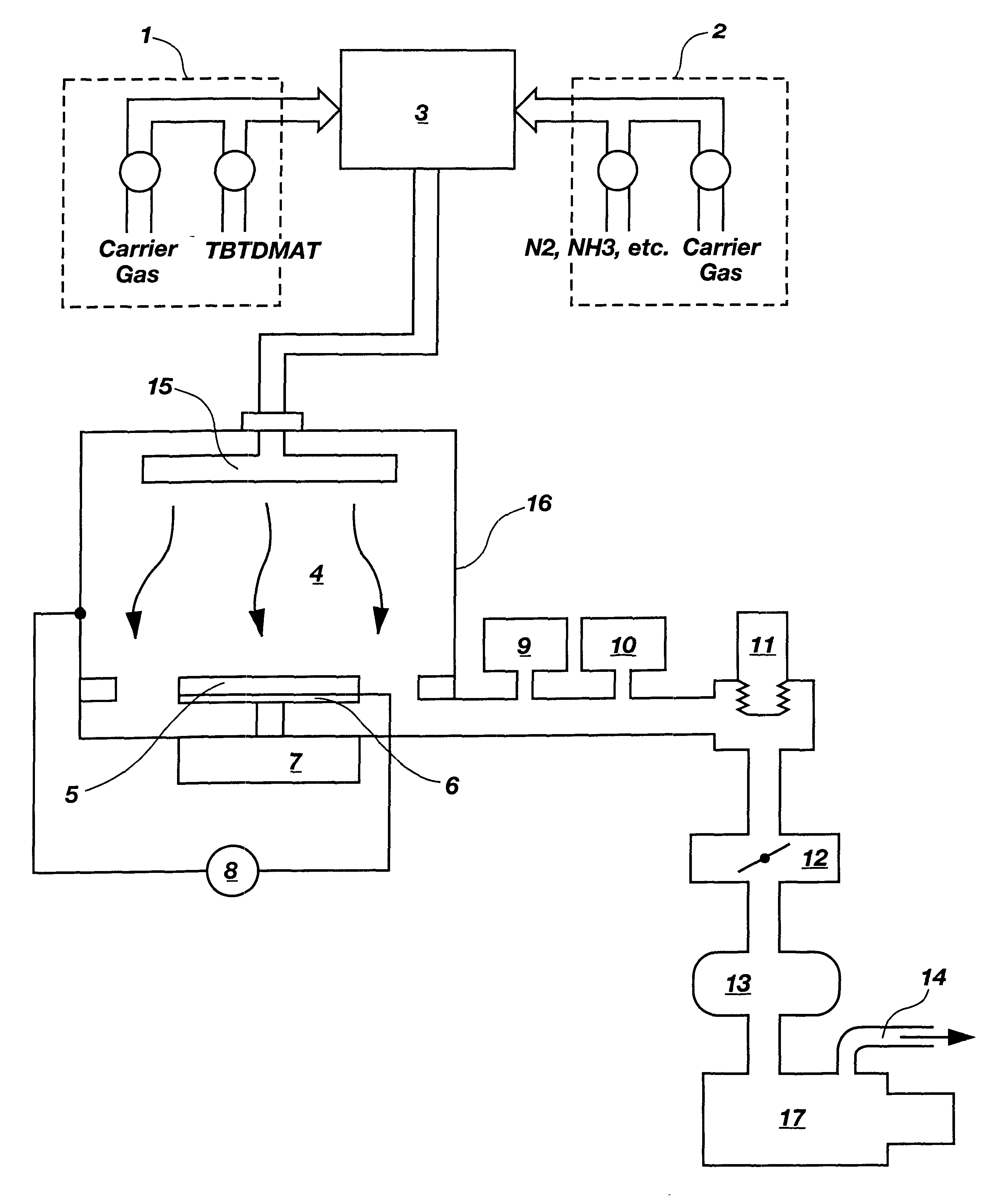
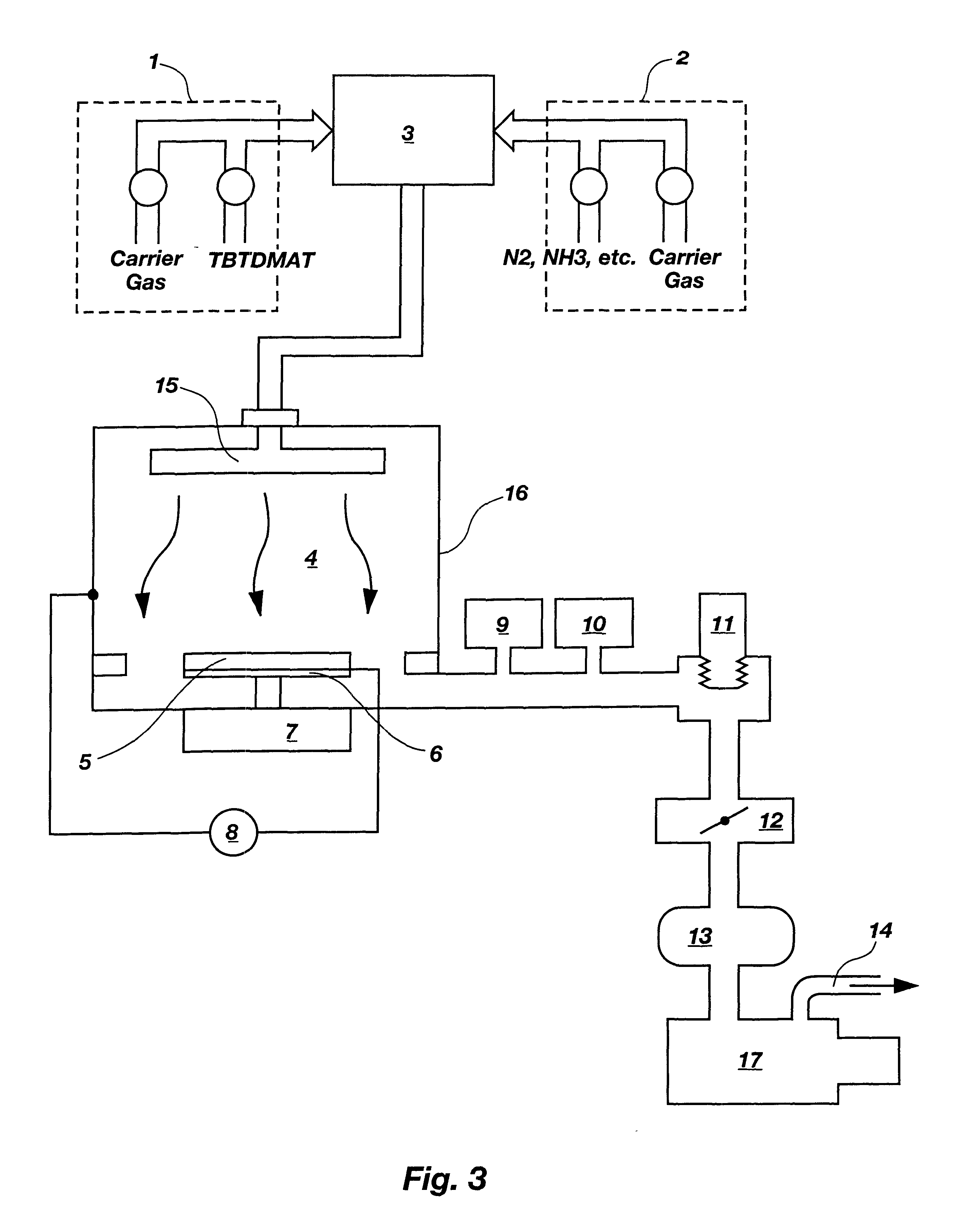
the invention which utilizes a cold-wall plasma enhanced chemical vapor deposition (PECVD) process will be described with reference to FIG. 3. Although the following description of the process represents what the inventor believe is the preferred embodiment of the process, the process may be practiced in either cold-wall or hot-wall plasma-enhanced chemical vapor deposition chambers, with or without premixing of the reactants. Furthermore, although the invention is directed to a technique for depositing conformal titanium nitride layers for use in the manufacture of integrated circuits, the process is also applicable to the deposition of titanium nitride on substrates other than semiconductor wafers.

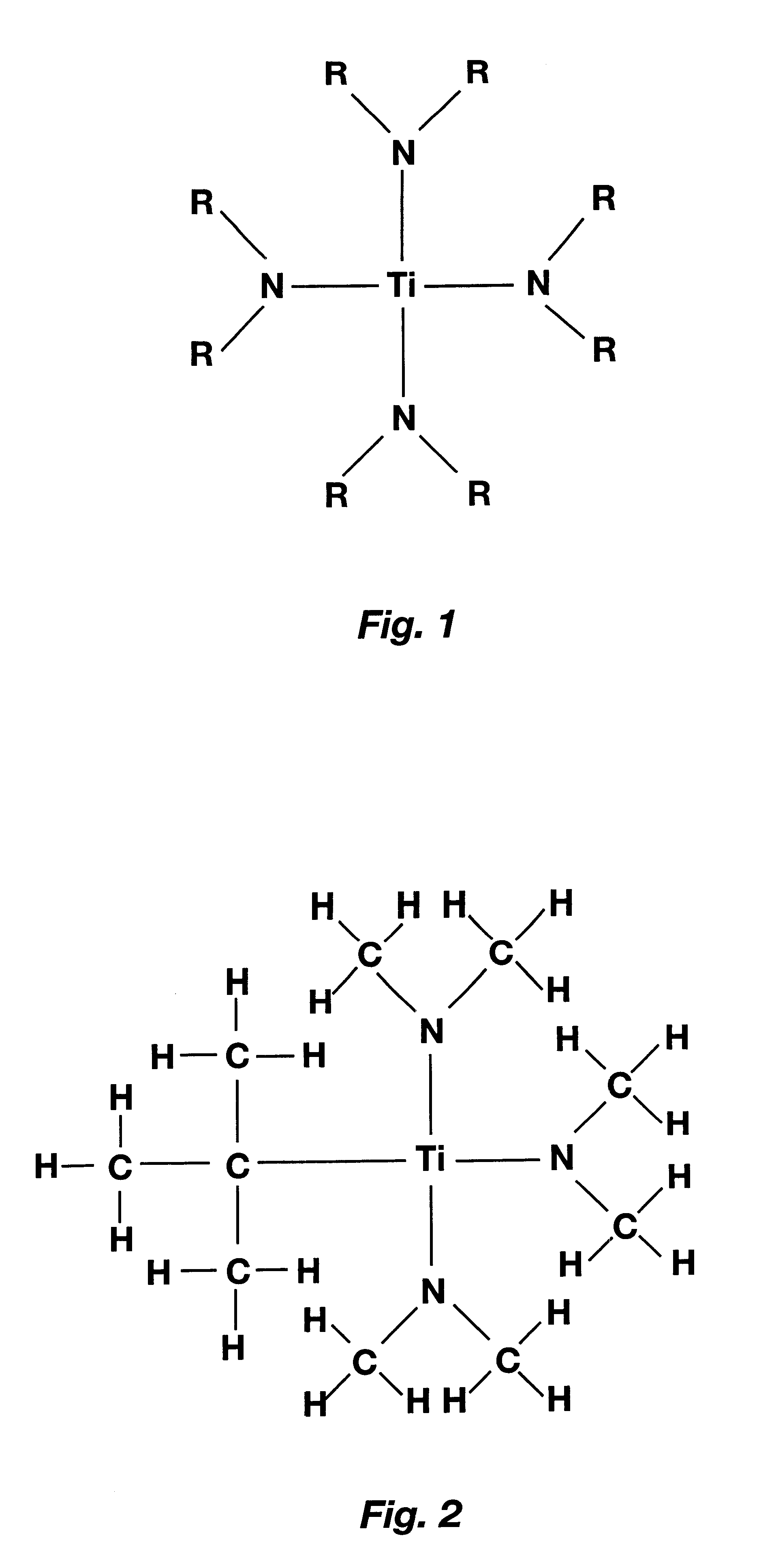
Referring now to FIG. 3, a tertiary-butyltris-dimethylamido-titanium metal-organic source gas is produced by heating liquid tertiary-butyltris-dimethylamido-titanium (the metal-organic precursor compound). The gas phase metal-organic compound transported by a carrier gas is admitted into...

second embodiment

A second embodiment of the invention will also be described with reference to the diagrammatic representation of the chemical vapor deposition chamber of FIG. 3. However, for this embodiment, no RF power is applied between the substrate holder 6 and the chamber wall 16. Instead, increased wafer temperature is relied on to effect a reaction between the tertiary-butyltris-dimethylamido-titanium and the nitrogen-containing gas. Diatomic nitrogen gas, because its dissociation temperature is greater than temperatures compatible with semiconductor processing, is not used for the process. Except for the use of higher temperatures within a range of about 500.degree. C. to 700.degree. C. and the lack of a plasma-generating RF power, other features of the process remain the same.

Other materials may be simultaneously incorporated in the titanium nitride films during either embodiment of the deposition process as heretofore described. For example, a titanium nitride film incorporating aluminum ...


PUM

PropertyMeasurementUnit
sheet resistanceaaaaaaaaaa
temperatureaaaaaaaaaa

Abstract

A process for depositing titanium nitride films containing less than 5% carbon impurities and less than 10% oxygen impurities by weight via chemical vapor deposition is disclosed. Sheet resistance of the deposited films is generally be within a range of about 1 to 10 ohms per square. The deposition process takes place in a deposition chamber that has been evacuated to less than atmospheric pressure and utilizes the organometallic compound tertiary-butyltris-dimethylamido-titanium and a nitrogen source as precursors. The deposition temperature, which is dependent on the nitrogen source, is within a range of 350° C. to 700° C. The low end of the temperature range utilizes nitrogen-containing gases such as diatomic nitrogen, ammonia, hydrazine, amides and amines which have been converted to a plasma. The higher end of the temperature range relies on thermal decomposition of the nitrogen source for the production of reaction-sustaining radicals. In such a case, the use of diatomic nitrogen gas is precluded because of its high dissociation temperature. Other materials may be simultaneously incorporated in the titanium nitride films during either embodiment of the deposition process as heretofore described. For example, a titanium nitride film incorporating aluminum and having the general formula TiAIN may be deposited by introducing aluminum-containing compounds. Additionally, a titanium nitride film incorporating tungsten and having the general formula TiNW may be deposited by introducing tungsten-containing compounds.

Description

1. Field of the InventionThis invention relates to integrated circuit fabrication technology and, more specifically, to processes for depositing titanium nitride films via chemical vapor deposition.2. Description of Related ArtThe compound titanium nitride (TiN) has numerous potential applications because it is extremely hard, chemically inert (although it readily dissolves in hydrofluoric acid), an excellent conductor, possesses optical characteristics similar to those of gold, and has a melting point around 3000.degree. C. This durable material has long been used to gild inexpensive jewelry and other art objects. However, during the last ten to twelve years, important uses have been found for TiN in the field of integrated circuit manufacturing. Not only is TiN unaffected by integrated circuit processing temperatures and most reagents, it also functions as an excellent barrier against diffusion of dopants between semiconductor layers. In addition, TiN also makes excellent ohmic co...

Claims


Application Information

Patent Timeline
Patent Type & Authority Patents(United States)
IPC IPC(8): C23C16/34
CPCC23C16/34
Inventor AKRAM, SALMAN
Owner MICRON TECH INC
Why Eureka
Try Eureka