Semi-insulating silicon carbide without vanadium domination

a silicon carbide and silicon carbide technology, applied in the direction of polycrystalline material growth, crystal growth process, after-treatment details, etc., can solve the problems of reducing yield, negatively affecting the crystalline quality of the resulting material, and generally too conductive silicon carbide grown by most techniques, etc., to achieve high frequency operation

Inactive Publication Date: 2002-05-28
CREE INC
View PDF23 Cites 99 Cited by
  • Summary
  • Abstract
  • Description
  • Claims
  • Application Information

AI Technical Summary

Benefits of technology

Therefore, it is an object of the present invention to provide a semi-insulating silicon carbide substrate without characterizing particular dopants as being universally "deep" or "shallow," and to provide a semi-insulating silicon carbide substrate that offers the capabilities that are required and advantageous for high frequency operation, but while avoiding the disadvantages of prior materials and techniques.
By avoiding the use of such elements, the invention likewise eliminates the need to compensate such elements with other elements and correspondingly reduces the complications that such compensation introduces into the crystal growth processes.
In such a preferred embodiment, the silicon carbide is grown under conditions that reduce the active nitrogen concentration to the point at which a relatively small amount of boron, preferably about 1E15 of boron, will make the crystal p-type. By controlling the growth conditions, the point defect concentrations can be brought to about 5E15 thus over-compensating the boron and producing the semi-insulating crystal. By reducing the concentration of nitrogen, and the corresponding compensating amounts of boron, the invention avoids the earlier-mentioned disadvantages of transition-metal domination and heavier degrees of doping and compensation. Because crystal growth of SiC is a relatively sophisticated process, exact parameters can differ depending on local or individual circumstances such as the particular temperatures used within the appropriate ranges and the characteristics of the equipment being used. Nevertheless, based on the disclosures herein, those of ordinary skill in this art can be expected to practice the invention successfully, and without undue experimentation.

Problems solved by technology

As recognized by those familiar with microwave devices, they often require high resistivity ("semi-insulating") substrates for coupling purposes because conductive substrates tend to cause significant problems at microwave frequencies.
As those familiar with silicon carbide are aware, however, silicon carbide grown by most techniques is generally too conductive for these purposes.
First, the presence of electronically significant amounts of any dopant, including vanadium, can negatively affect the crystalline quality of the resulting material.
As a second disadvantage, the introduction of compensating amounts of vanadium can reduce the yield and add expense to the production of semi-insulating silicon carbide substrates.
Third, the proactive compensation of silicon carbide, or any other semiconductor element, can be somewhat complex and unpredictable and thus introduces manufacturing complexity that can be desirably avoided if the compensation can be avoided.

Method used


Image

  • Semi-insulating silicon carbide without vanadium domination
  • Semi-insulating silicon carbide without vanadium domination
  • Semi-insulating silicon carbide without vanadium domination

Examples


Embodiment Construction

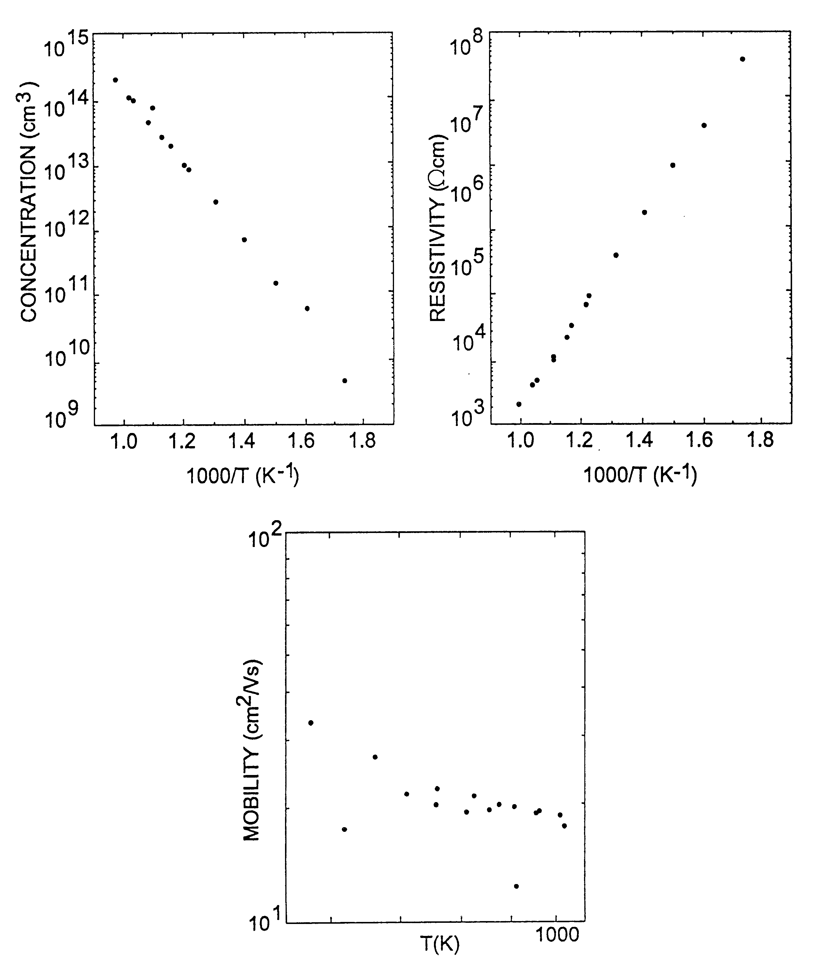
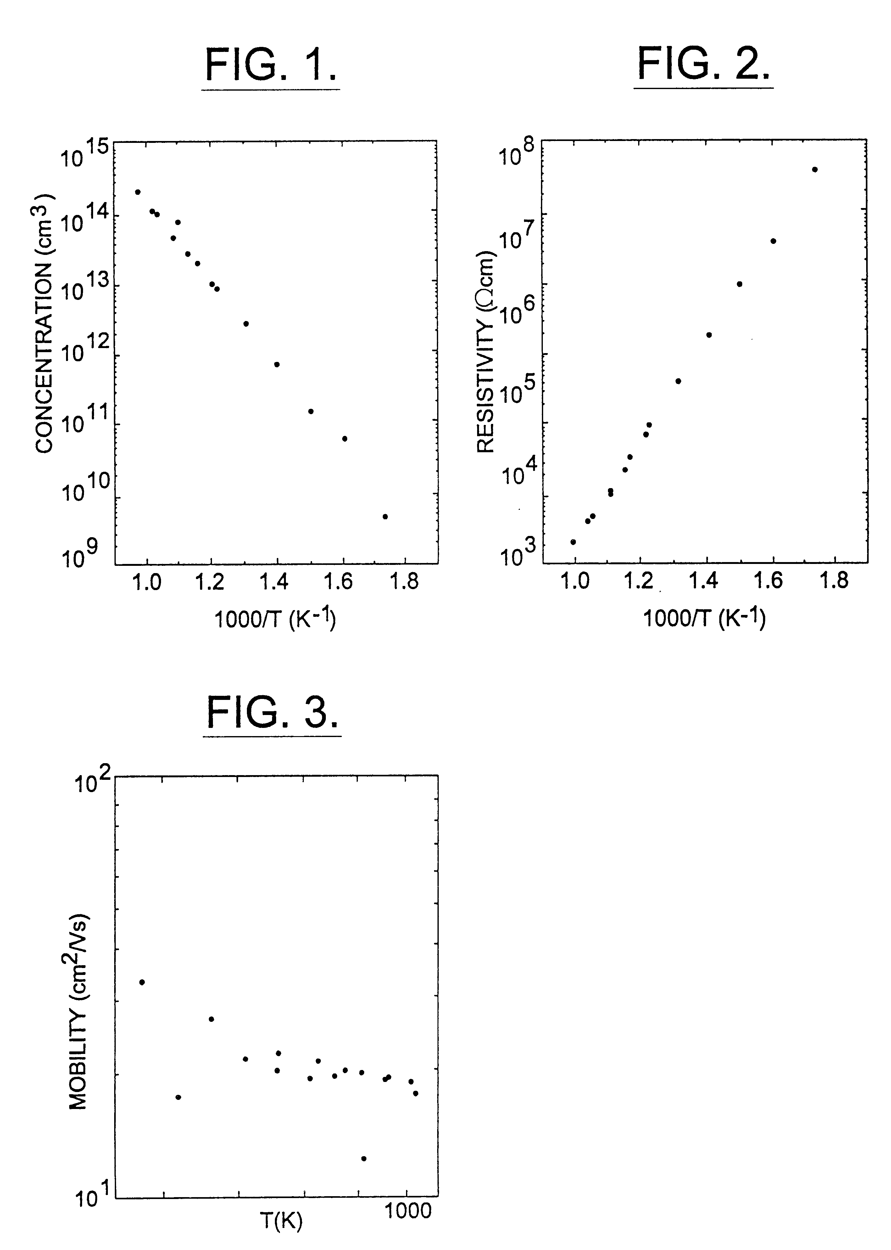
Two wafers of semi-insulating SiC were examined at the Air Force Research Laboratory at Dayton, Ohio (Wright-Patterson Air Force Base), with high temperature Hall effect and SIMS. No understandable results were available from one of the wafers (possibly because of unsatisfactory ohmic contacts), but two Hall samples from the second wafer both gave the same results, giving a reasonable confidence level in those results.

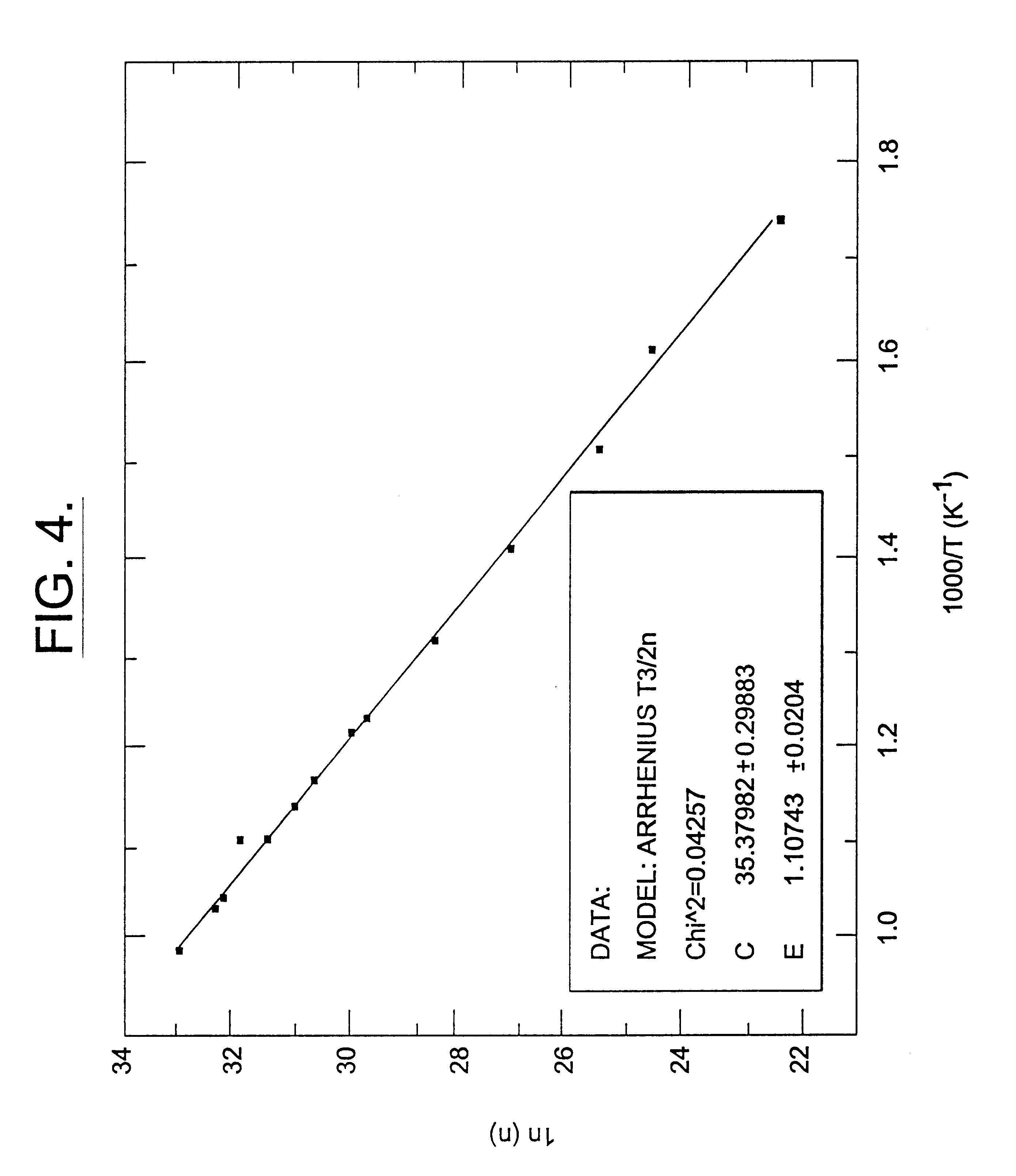
Both wafers were insulating at room temperature. The measurable wafer was thermally activated at elevated temperatures and the carrier concentration was measurable, which is not always possible in semi-insulating material because of the low mobilities due to the high temperatures involved. The carrier concentration was around 10.sup.15 cm.sup.-3 at 1000K where the resistivity was about 103 .OMEGA.-cm. Such carrier concentration is about one to two orders of magnitude lower than that seen in conventional semi-insulating material or vanadium doped material at the same te...


PUM

PropertyMeasurementUnit
wavelengthsaaaaaaaaaa
atomic massaaaaaaaaaa
carrier concentrationaaaaaaaaaa

Abstract

A semi-insulating bulk single crystal of silicon carbide is disclosed that has a resistivity of at least 5000 OMEGA-cm at room temperature and a concentration of trapping elements that create states at least 700 meV from the valence or conduction band that is below the amounts that will affect the resistivity of the crystal, preferably below detectable levels. A method of forming the crystal is also disclosed, along with some resulting devices that take advantage of the microwave frequency capabilities of devices formed using substrates according to the invention.

Description

The term "microwaves" refers to electromagnetic energy in frequencies covering the range of about 0.1 gigahertz (GHz) to 1,000 GHz with corresponding wavelengths from about 300 centimeters to about 0.3 millimeters. Although "microwaves" are perhaps most widely associated by the layperson with cooking devices, those persons familiar with electronic devices recognize that the microwave frequencies are used for a large variety of electronic purposes and in corresponding electronic devices, including various communication devices, and the associated circuit elements and circuits that operate them. As is the case with many other semiconductor electronic devices and resulting circuits, the ability of a device (or circuit) to exhibit certain desired or necessary performance characteristics depends to a large extent, and often entirely, upon the material from which it is made. One appropriate candidate material for microwave devices is silicon carbide, which offers a primary advantage for m...

Claims


Application Information

Patent Timeline
Patent Type & Authority Patents(United States)
IPC IPC(8): C30B23/00C30B33/00H01L29/02H01L29/24H01L29/78H01L29/778H01L29/66H01L29/812C30B29/36H01L21/338H01L29/161
CPCC30B23/00C30B33/00H01L29/1608C30B29/36H01L29/778H01L29/78H01L29/812H01L31/0312
Inventor CARTER, JR., CALVIN H.BRADY, MARKTSVETKOV, VALERI F.
Owner CREE INC
Why Eureka
Try Eureka