Curable sheet for circuit transfer

a technology of curable sheets and circuits, applied in electrical devices, metal layered products, metal pattern materials, etc., can solve the problems of difficult high-density interconnection, limit circuit design, and essentially difficult to heighten yield, and achieve the effect of simplifying the multiplayer lamination

Inactive Publication Date: 2002-09-24
ASAHI KASEI E-MATERIALS CORPORATION +1
View PDF7 Cites 21 Cited by
  • Summary
  • Abstract
  • Description
  • Claims
  • Application Information

AI Technical Summary

Benefits of technology

Other objects and effects of the invention will become more apparent from the following description.
As a result of the extensive investigation on the above-described objects, the present inventors found that by transferring a wiring circuit to a curable sheet for circuit transfer, which contains a thermosetting polyphenylene ether resin composition having a specific composition, from a transfer base material, curable insulating layers stacked one after another can be cured in one step, leading to simplification of the multiplayer lamination, and that the conductor resistance varies largely not only by the penetration of oxygen or moisture from the outer circumstances, which has so far been

Problems solved by technology

The conventional multilayer printed wiring board however cannot satisfy such a demand because in such a wiring board, interlayer connection is attained by plating inside of a thorough-hole formed to penetrate through a substrate so that this through-hole imposes a limitation on circuit designing and makes it difficult to accomplish high-density interconnection.
In this build-up process, however, layers are formed not simultaneously but successively so that a yield of the finished product corresponds to the multiplication product of the yields of successively formed layers, making it essentially difficult to heighten the yield.
In addition, a build-up substrate using a photosensitive resin is accompanied with the problem that introduction of a photosensitive group into the resin lowers heat resistance or water absorption resistance of the substrate, which makes it impossible to satisfy the performances required for it in near future as a semiconductor device package.
At an amount of Component (B) less than 45 parts by weight, sufficient adhesion properties necessary for transfer are not available upon thermal softening of the resin and transfer of a wiring circuit layer made of a metal foil from a transfer base material to an insulating layer, leading to a transfer failure.
Amounts exceeding 55 parts by weight, on the other hand, soften the resin too much and excessively increases its fluidity, causing misregistration of the wiring transferred to the insulating layer.
At an amount of Component (C) less than 25 parts by weight, the uncured material has low strength, which causes inconveniences such as tearing of the material upon handling.
At an amount exceeding 35 parts by weight, on the other hand, sufficient adhesion properties necessary for transfer are not available upon thermal softening of the resin and transfer of a wiring circuit layer made of a metal foil from a transfer base material to an insulating layer, leading to transfer failure.
% cause lowering in the strength and heightening of the thermal expansion coefficient of the resulting insulating layer or multilayer wiring board so that they are unsatisfactory.
%, on the other hand, cause breakage of the sheet, thereby causing inconveniences upon sheet formation which will be described later.
The present inventors found that impurities contained in the brominated flame retardant induce oxidation of the surface of the metal powder in a conductive paste constituting a wiring conductor for for

Method used


Image

  • Curable sheet for circuit transfer
  • Curable sheet for circuit transfer
  • Curable sheet for circuit transfer

Examples


example 1

The above-described modified polyphenylene ether resin, hydrogenated block copolymer, triallyl isocyanurate and, as a bromine flame-retardant, Saytex BT-93W were added, at the composition as shown in Table 2, to toluene of 80.degree. C., followed by stirring for 1 hour to dissolve the former in the latter. A polymerization initiator was added at the composition as shown in Table 2. Then, silica was added at the composition as shown in Table 2 to disperse it in the mixture, whereby the corresponding varnish was prepared. The resulting varnish was applied to a PET film of 100 .mu.m thick by a blade coater, followed by drying in an air oven at 50.degree. C. for 30 minutes. Then, the PET film was peeled, whereby a curable sheet of 100 .mu.m thick was prepared. A through-hole of 0.1 mm in diameter was made in the thus-prepared curable sheet by a CO.sub.2 gas laser. A conductive paste containing silver-plated copper particles was filled in the through-hole to form a via-hole conductor.

An ...

examples 2 to 4

In a similar manner to Example 1 except that the composition ratio of each of the modified polyphenylene ether resin, hydrogenated block copolymer, triallyl isocyanurate, brominated flame retardant, silica and polymerization initiator was changed as shown in Table 2, a multilayer wiring board was produced.

As a result of observation of the cross-section of the multilayer wiring board thus formed at the position near the wiring circuit layer or via-hole conductor, it has been found that the wiring circuit layer formed by transfer was embedded in the insulating layer enough to form a flat surface and that the wiring circuit layer and via-hole conductor were connected well. As a result of the continuity test between interconnects, no disconnection was recognized.

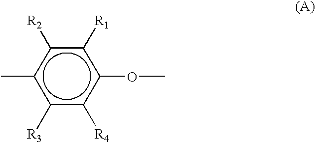
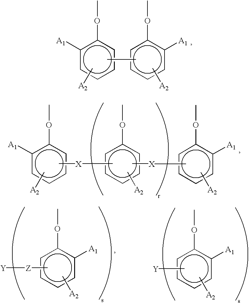
The unit of each of the above-described components other than spherical silica is parts by weight based on 100 parts by weight of (A)+(B), while that of spherical silica is vol. % based on the whole amount. Modified PPE resin: m...

example 5

In toluene of 80.degree. C., were dissolved 50 parts of the above-described modified polyphenylene ether resin and 50 parts by weight of triallyl isocyanurate. To the resulting solution, successively added were 25 parts by weight of Saytex 8010 (trade name; product of Albemarle Corporation) as a flame retardant and 6 parts by weight of "Perhexyne 25B" as a polymerization initiator, whereby a varnish formed of the resulting polyphenylene ether resin composition was formed. A glass cloth was impregnated with the varnish, followed by drying in an air oven to form a composite prepreg.

A through-hole was made in the prepreg by a CO.sub.2 gas laser. After a conductive paste containing a silver-plated copper powder was filled in the hole as in Examples 1 to 4, a wiring circuit layer made of the copper foil was formed by transfer, whereby one wiring layer unit was obtained.

Three wiring layers were stacked one after another. A curable sheet having the composition similar to that prepared in E...


PUM

PropertyMeasurementUnit
Percent by massaaaaaaaaaa

Abstract

Provided is a curable sheet for the formation of a wiring circuit layer by circuit transfer from a transfer base material, wherein the curable sheet comprises (A) a reaction product between a polyphenylene ether resin and an unsaturated carboxylic acid or acid anhydride, (B) triallyl isocyanurate and/or triallyl cyanurate, (C) a hydrogenated block copolymer obtained by hydrogenation of a block copolymer comprising at least one polymer block A mainly comprising an aromatic vinyl compound and at least one polymer block B mainly comprising a conjugated diene compound, and (D) an inorganic filler; said Component (A), Component (B) and Component (C) being contained in amounts of 45 to 55 parts by weight, 55 to 45 parts by weight, and 25 to 35 parts by weight, respectively, each based on 100 parts by weight of total of Components (A) and (B), and said Component (C) being contained in an amount of 20 to 80 vol. %.

Description

The present invention relates to a curable sheet to be used for the formation of a wiring circuit layer by the transfer from a transfer base material, and to a multilayer wiring board using a cured sheet as an insulating layer, which has been obtained by curing the above-described curable sheet, for example, a multilayer wiring board suitable for use as a semiconductor device package. The present invention also relates to a process for producing the above-described multilayer wiring board.RELATED ART OF THE INVENTIONAs a wiring board, for example, a multilayer wiring board used as a semiconductor device package, a multilayer printed wiring board produced by adhering a copper foil onto the surface of each of insulating substrates including a resin, etching the copper foil to form a minute circuit and then stacking the resulting substrates one on top of the other has been proposed conventionally and employed in practice. Recently, there is a demand for the development of a multilayer ...

Claims


Application Information

Patent Timeline
IPC IPC(8): C08L71/12C08K5/00C08L71/00C08K5/3492H05K3/20H05K1/03C08L25/00C08L25/10H05K3/46H05K3/40
CPCC08K5/34924C08L71/126H05K1/0373H05K3/20Y10T428/24917H05K3/4069H05K3/4626H05K3/4652H05K3/4655H05K2201/012H05K2201/0209C08L25/10C08L2666/24
Inventor KINOSHITA, SHOZOYAMAMOTO, MASAKIHAYASHI, KATSURAHORI, MASAAKIFUJII, TOSHIKAZU
Owner ASAHI KASEI E-MATERIALS CORPORATION
Why Eureka
Try Eureka