Ion implanters, however, are among the most sophisticated and complex systems in semiconductor manufacturing.
For example, ion implantation systems may introduce a number of defects (e.g., non-uniformities) into the semiconductor process.
Such defects may cause significant yield problems.
The accumulation of contaminants over time may adversely affect the performance of the ion implanter and may reduce the
wafer yield below acceptable levels.
Accurate measurement of the
implant dose, however, may be a difficult task because the measurement is generally based on integrating the beam current.
The test may also be performed at several different current levels because testing at an improper current may cause the forward and reverse test results to differ or to cause the readings to drift.
During this processing, masking materials such as
photoresist may volatilize or reflow which may cause
contamination or removal problems in subsequent processing.
Consequently, the time required to perform these additional processing steps increases the processing time and cost associated with
electrical testing.
Furthermore, long test times may be extremely costly if additional wafers have been processed incorrectly before the electrical test results were available.
Suspending processing until the electrical test results are available, however, may also be costly due to production delays and idle production tools.
Scan lock-up is a common problem which may result from overlap of individual
Gaussian beam traces and may cause
dopant non-uniformities across the wafer.
Scan lock-up may be particularly problematic at low
dopant doses.
For example, low dopant doses typically have decreased beam currents and scan times which may lead to significant overlap in some regions of the wafer and
doping level gaps in other regions of the wafer.
Positive charge build-up on an insulating layer on the wafer may also result in non-linear scanning because the build-up may alter the charge balance in the
ion beam and lead to significant
dose variations across the wafer.
Loss of
beam diameter control, or defocusing, is another common problem in ion implantation which may result from separation of the beam due to repulsion of like charges.
Defocusing of the beam may also cause uneven
ion density and non-uniform
implant concentrations in the wafer.
There are several disadvantages, however, in using the optical
dosimetry technique to monitor ion implantation processes.
For example, because only a
photoresist-coated transparent substrate may be used in this technique, additional processing steps and materials are typically required.
Furthermore, the testing method may not accurately predict the ion implantation performance of a product wafer which may have a
topography which differs dramatically from a substrate coated with a planar
resist layer.
For example, positive charge build-up on a wafer may be particularly problematic when implanting into an insulating layer, such as
resist or
silicon dioxide, which may lead to significant
dose variations across the wafer.
The
topography or patterning of the masking layer on a product wafer may cause additional localized positive charge build-up.
A wafer having a planar
resist layer may not accurately show the localization of positive charge build-up.
Therefore, using a dissimilar test wafer may not accurately detect all of the potential problems that may occur in an ion implantation process.
There are several disadvantages, however, to using the modulated and non-modulated reflectance technique as a
process control method for ion implantation.
Therefore, this approach may not be particularly useful when the index of
refraction of the material is not accurately known.
The implantation of ions into the masking material may cause physical damage and chemical changes in the masking material.
A semiconductor substrate may also experience significant damage due to the implantation of ions into regions of the semiconductor substrate.
For example, damage to the
silicon by the implanted ions may produce an amorphous layer below an upper crystalline damaged layer.
Chemical changes and physical damage to the masking material may occur due to incorporation of the dopant ions.
For example, the upper portion of the masking material may undergo physical damage due to the collisions of the
high energy ions with the upper surface of the masking material.
The implantation of ions into the masking material may cause physical damage to the upper surface of the masking material and may reside in the middle portion of the masking material.
Higher energy implantation processes may cause more damage to an upper portion of the masking material and drive the ions farther into the masking material than low energy ion implantation process.
For example, a masking material may have a
high absorption over a range of wavelengths and may not reflect enough light in this range of wavelengths to be detected by conventional means.
The cauchy model, however, may not be valid for wavelengths at which a material exhibits absorption.
During ion implantation processes, and especially in processes using
high dosage levels, the semiconductor substrate may also experience significant damage due to the implantation of dopant ions into regions of the semiconductor substrate.
The damage in the upper crystalline layer may be caused, for example, by electronic collisions between atoms of the
silicon layer and the implanted ions.
Displacement damage, however, may not be produced if the ions entering the silicon layer do not have enough energy per nuclear collision to displace silicon atoms from their lattice sites.
Damage to the silicon by the implanted ions may produce an amorphous layer below the upper crystalline damaged layer.
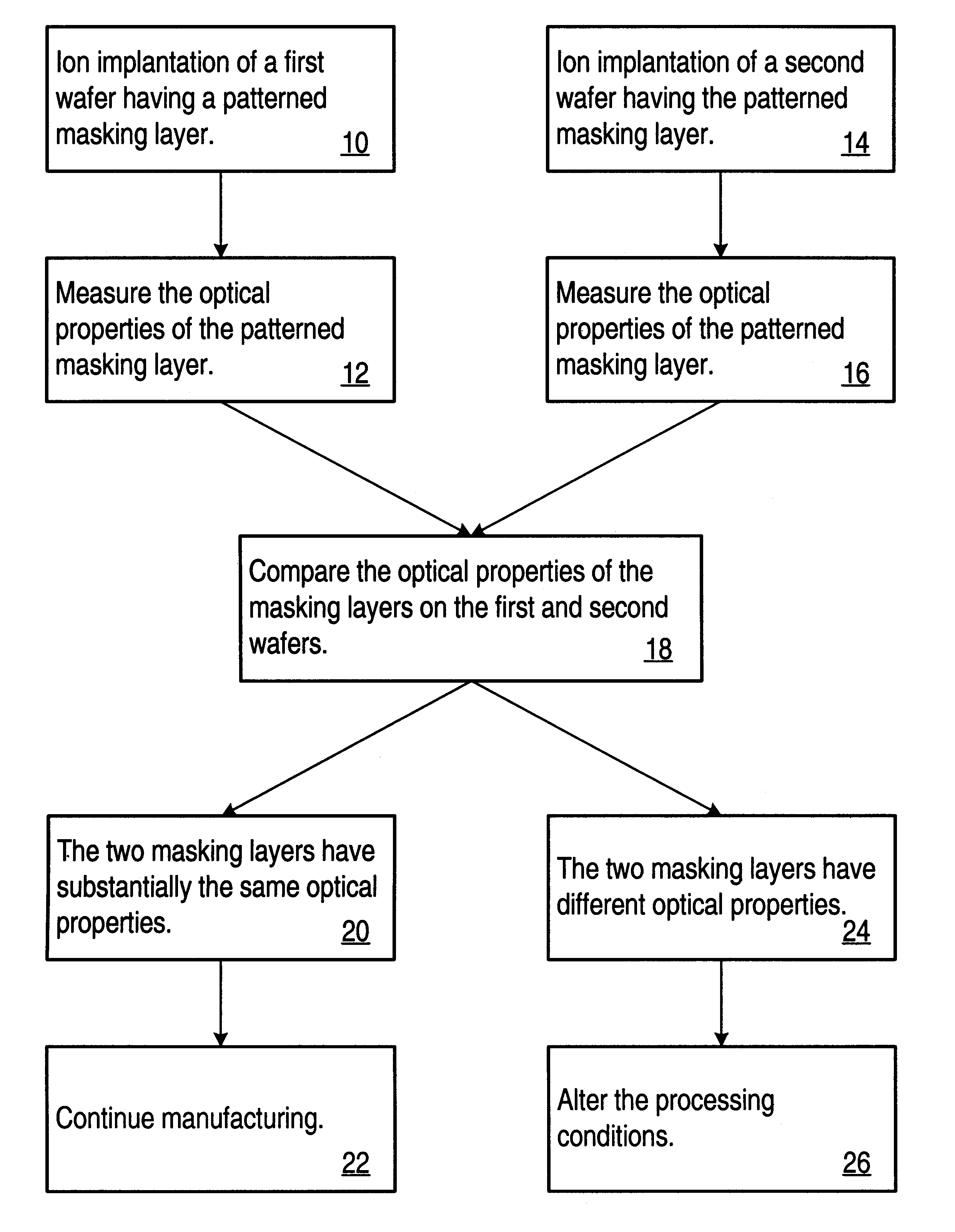
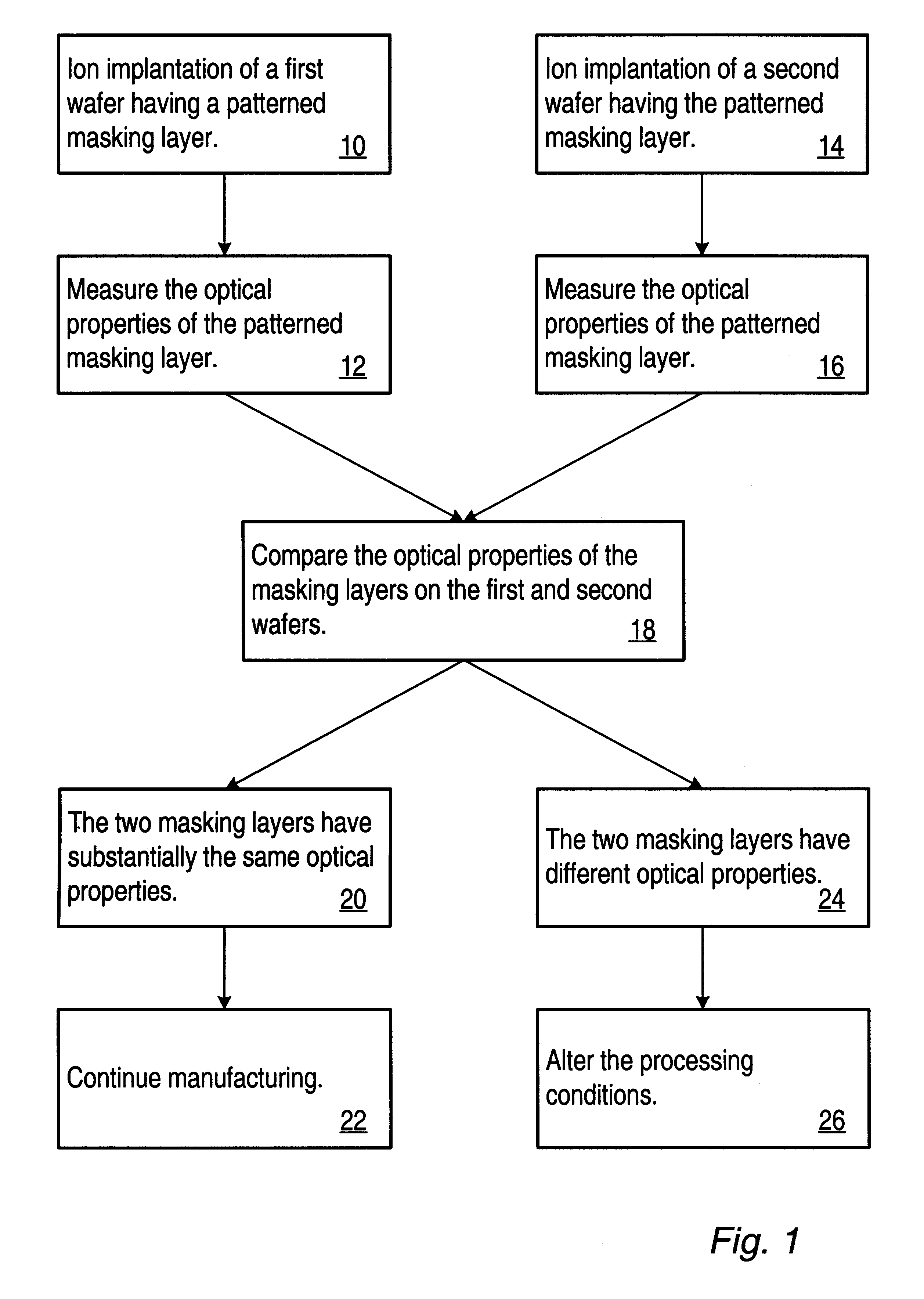
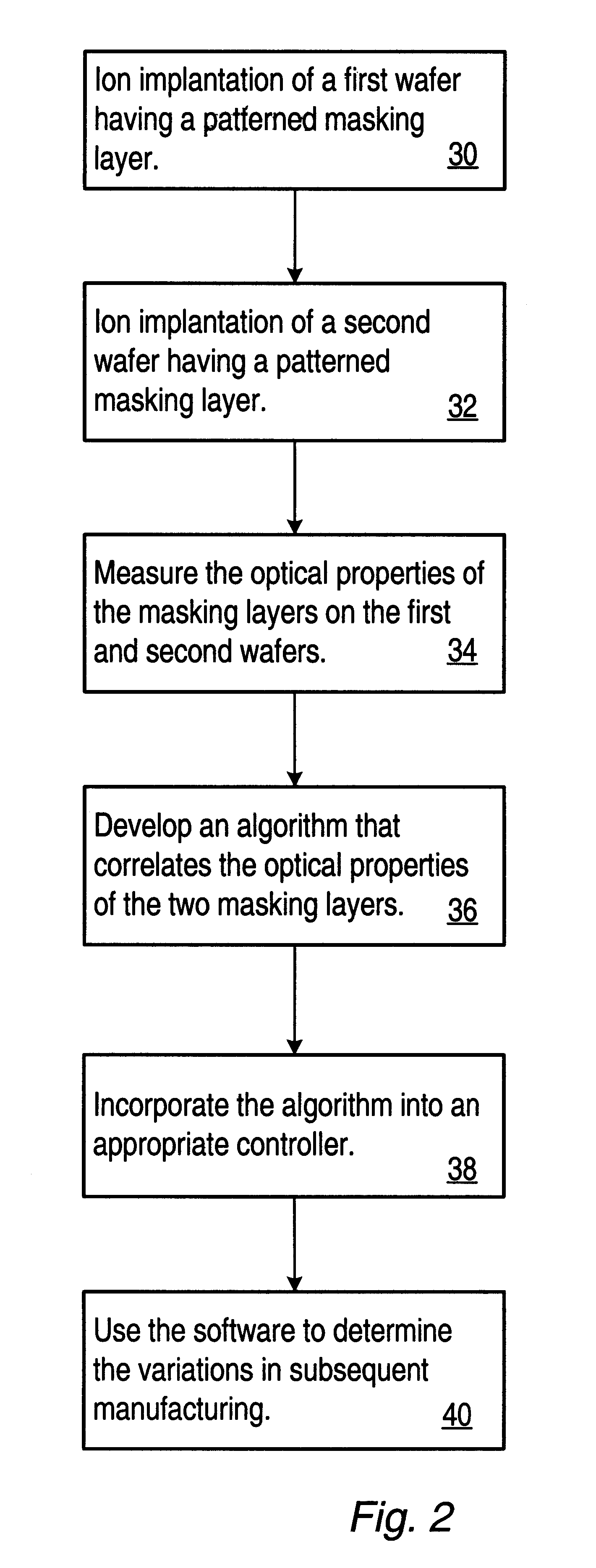
Although the same process parameters may be used for the production of the product and reference wafers, over time the produced
process conditions may begin to drift outside of a design tolerance for the ion implantation process.
This drift may occur despite using the same operating parameters for the ion implantation instrument.
For an ion implantation process, this drift may be due to contamination, beam
neutralization, secondary-
electron emission, or scan lock-up.
Therefore, drift in the performance of a tool alone may be large enough to cause an ion implantation process or device to be outside of the design tolerance and may significantly reduce the yield of working semiconductor devices.
Similarly, fabricating monitor wafers requires time and money resources that may be saved if evaluation of semiconductor manufacturing processes may be done using non-sacrificial product wafers.
In this manner, the number of incorrectly processed product wafers may also be reduced which may result, in turn, in a higher manufacturing yield and lower manufacturing costs.

