Magnetically enhanced inductively coupled plasma reactor with magnetically confined plasma

a plasma reactor and magnetically enhanced technology, applied in the direction of plasma technique, chemical vapor deposition coating, coating, etc., can solve the problems of contaminating the process, destroying affecting the integrity of the process,

Inactive Publication Date: 2002-10-29
APPLIED MATERIALS INC
View PDF20 Cites 85 Cited by
  • Summary
  • Abstract
  • Description
  • Claims
  • Application Information

AI Technical Summary

Problems solved by technology

Such an approach for plasma confinement has several inherent problems where employed in plasma reactors for processing semiconductor wafers.
First, the walls confining the plasma are subject to attack from ions in the plasma, typically, for example, by ion bombardment.
Such attack can consume the material in the walls or introduce incompatible material from the chamber walls into the plasma process carried out on the wafer, thereby contaminating the process.
As one example, if the chamber walls are aluminum and the plasma process to be performed is plasma etching of silicon dioxide, then the material of the chamber wall itself, if sputtered into the plasma, is incompatible with the process and can destroy the integrity of the process.
Second, it is necessary to provide certain openings in the chamber walls and, unfortunately, plasma tends to leak or flow from the chamber through these openings.
Such leakage can reduce plasma density near the openings, thereby upsetting the plasma process carried out on the wafer.
The above problems are intensified in reactors capable of generating high density plasmas such as a Magnetically Enhanced Inductively Coupled Plasma reactor.
As the pedestal must be moved into the magnetic bucket, the bias power and cooling lines must follow which is not desirable.
As discussed above, a problem inherent to plasma reactors, including MEICP reactores, is degradation of reactor components exposed to the plasma.
Such attack can consume the material causing periodic maintenance and reactor down time.
In addition, the chamber wall may introduce an incompatible material into the plasma.
For example, if a silicon dioxide etch is being performed and the chamber walls are aluminum, the aluminum may sputter into the plasma and deposit on the workpiece, thereby contaminating the workpiece.
Likewise, any by-products deposited on the chamber walls may also sputter or flake off and contaminate the workpiece.
In addition to the surface of the walls, any openings, such as the opening for workpiece placement on the pedestal or the vacuum pump opening are also subject to degradation.
Such degradation may prevent those openings from functioning properly.
For example, the workpiece opening which is normally sealed during processing may not seal properly due to degradation and as a result, allow air to leak in thereby reducing plasma density and upsetting workpiece processing.
Likewise, the pumping opening may become obstructed thereby affecting pumping efficiency.
Another problem with this type reactor is that the magnetic bucket protects the sidewalls but not the top wall.
Because the plasma near the ceiling has very high density as it exits the plasma source chamber, the exposed ceiling experiences a greater degree of degradation by the plasma.
Furthermore, because the ceiling is unprotected, build-up is more likely to occur.
Build-up on the ceiling can change processing parameters and degrade processing.
In such a case, the coupling of bias power to the workpiece affects the ion energy.
Increasing bias power during processing, however, would further complicate processing and introduce uncertainties to processing.
Furthermore, the problem is exaggerated after several workpieces have been processed and more build-up is added to the anode.
Cleaning of the chamber after processing each workpiece is possible but not desirable because it would lower throughput and increase costs.
Changes in ion energy during processing results in different and often unacceptable etch characteristics.
For example, polymer build-up during an etch process could lead to etch stopping.
Therefore, the build-up of polymer during ion etch is particularly problematic.
A larger gap would cause the power density drops which would unacceptably lower the etch rate.
While high density plasma generally improves processing, it may also increase reactor component degradation.
Components such as the workpiece insertion opening and associated mechanisms, the vacuum pump opening and associated mechanisms, and the processing chamber walls, among other components, are susceptible to damage by the plasma.

Method used


Image

  • Magnetically enhanced inductively coupled plasma reactor with magnetically confined plasma
  • Magnetically enhanced inductively coupled plasma reactor with magnetically confined plasma
  • Magnetically enhanced inductively coupled plasma reactor with magnetically confined plasma

Examples


Embodiment Construction

Conventional Reactor Elements

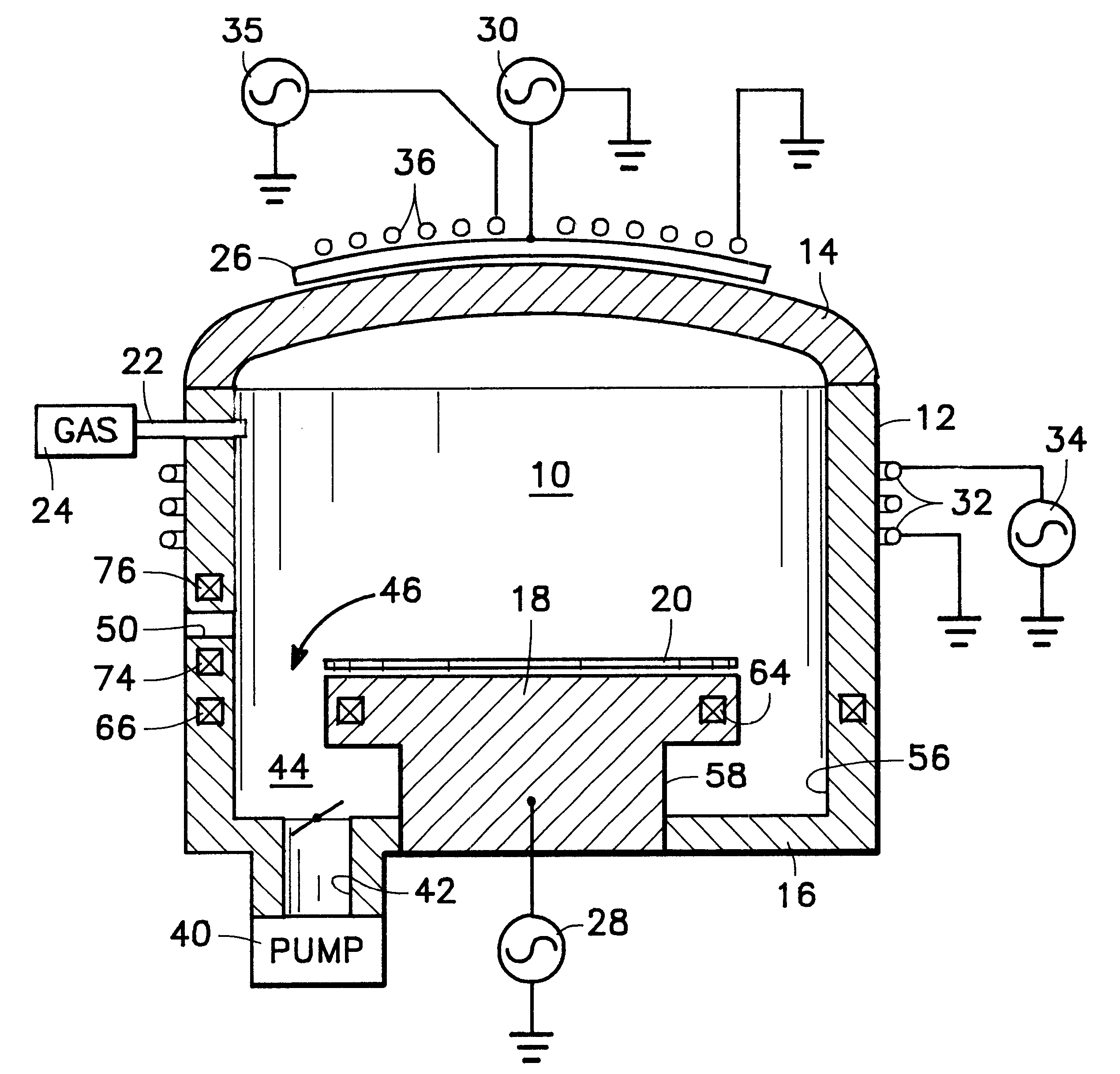
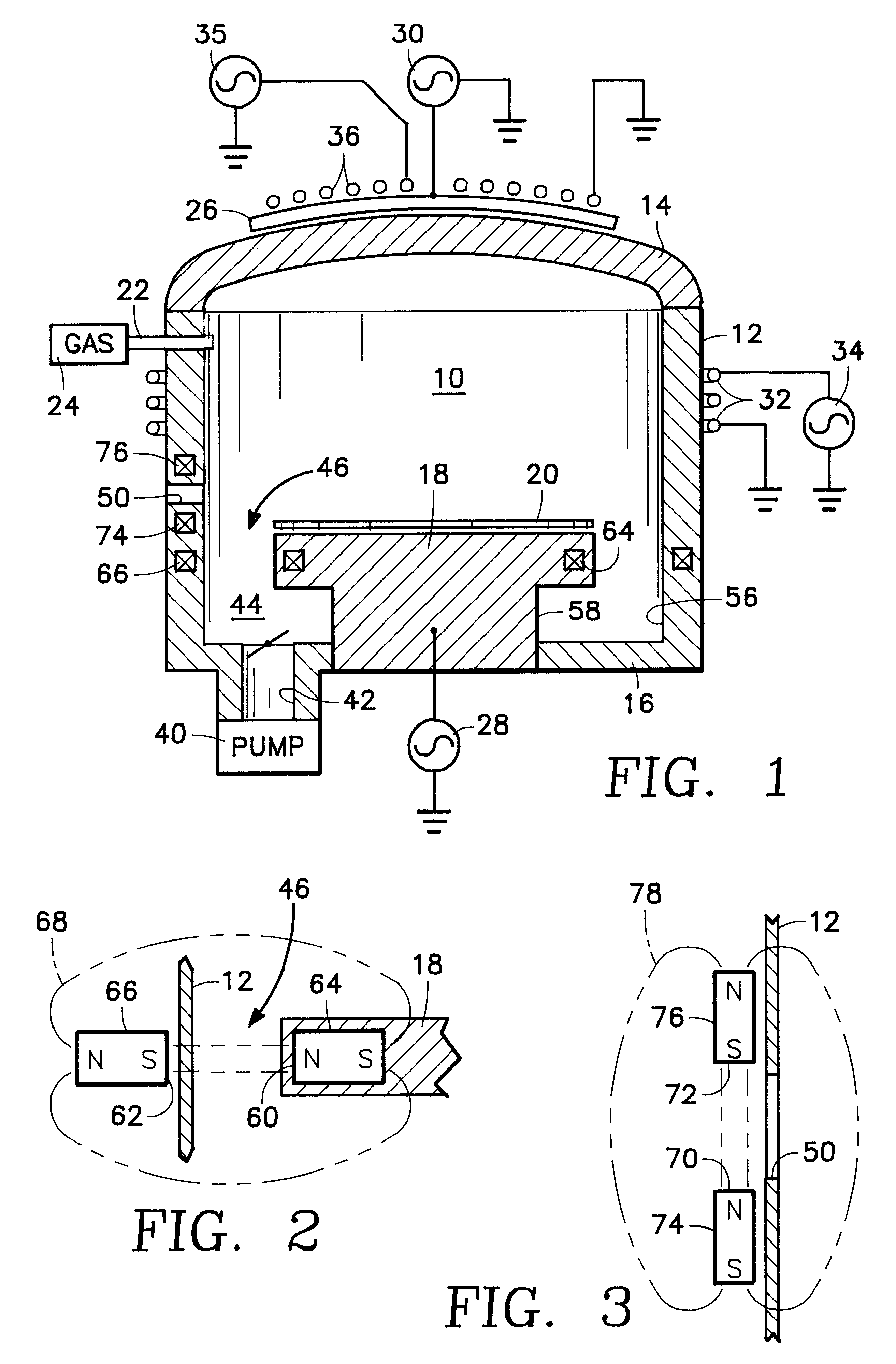
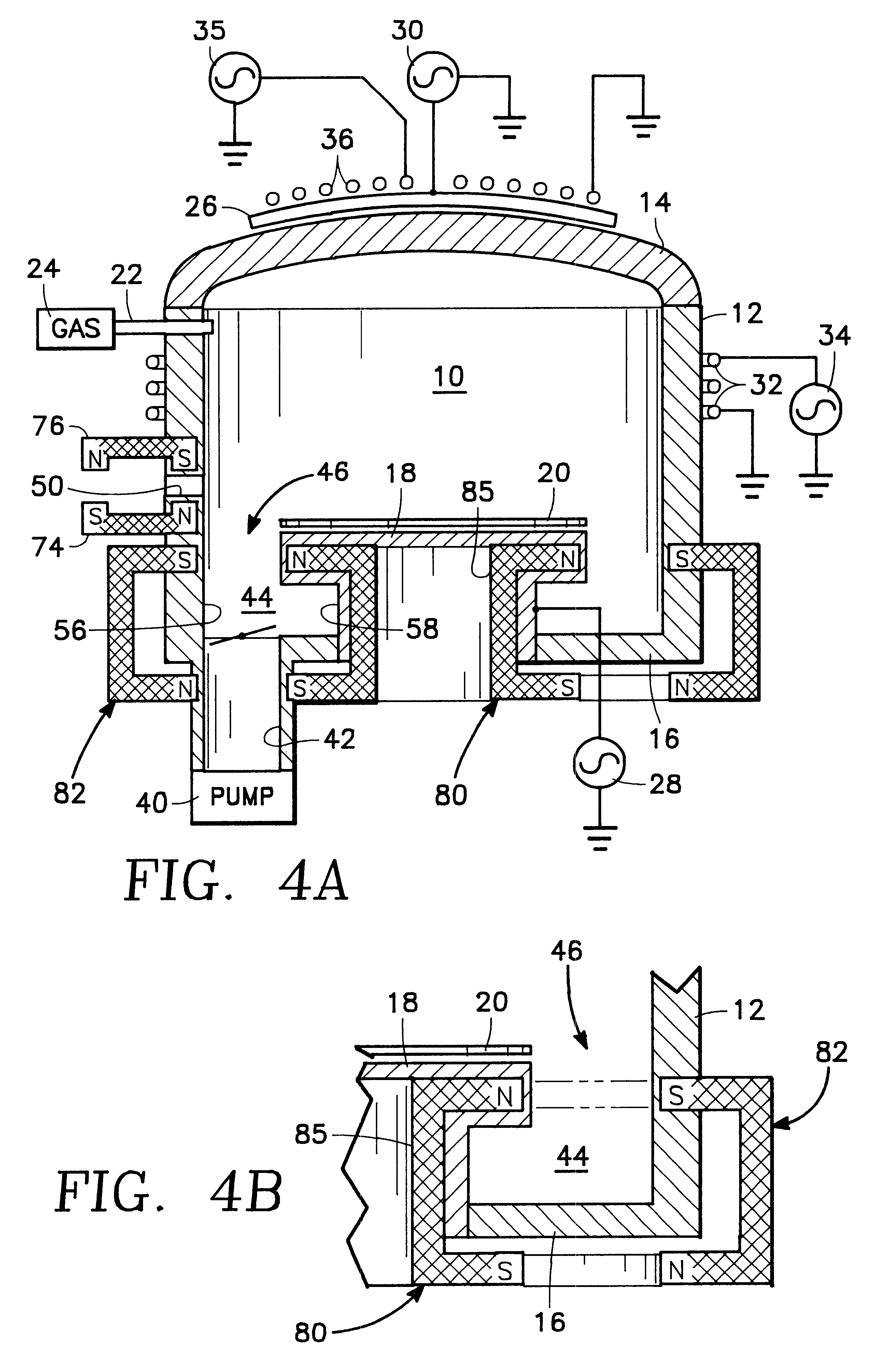
Referring to FIG. 1, an RF plasma reactor for processing a semiconductor wafer has a vacuum chamber 10 enclosed by a cylindrical side wall 12, a ceiling 14 and a floor 16. A wafer pedestal 18 supports a semiconductor wafer 20 which is to be processed. A plasma precursor gas is injected into the chamber 10 through a gas injector or inlet 22 from a gas supply 24. Plasma source power is coupled into the chamber 10 in any one of several ways. For example, the reactor may be a "diode" configuration, in which case RF power is applied across a ceiling electrode 26 and the wafer pedestal 18. This is accomplished by connecting the pedestal 18 and the ceiling electrode 26 to either one of two RF power sources 28, 30. Alternatively, a cylindrical side coil 32 wound around the chamber side wall 12 is connected to an RF power source 34. Alternatively to the foregoing, or in addition thereto, a top coil 36 is connected to an RF power supply. Although not shown in FIG....


PUM

PropertyMeasurementUnit
widthaaaaaaaaaa
widthaaaaaaaaaa
diameteraaaaaaaaaa

Abstract

The present invention provides a plasma reactor having a plasma source chamber capable of generating a high density plasma typically utilizing a helicon wave. The plasma is delivered to a process chamber having a workpiece. The present invention may provide a plurality of magnets, each being located longitudinally around an axis perpendicular to the plane of the workpiece to form a magnetic bucket that extends the length of the side wall of the processing chamber and across a workpiece insertion opening and a vacuum pump opening. The magnetic bucket of the present invention may be formed so that the pedestal need not be raised to be within the bucket, or may be formed by permanent magnets oriented with one pole of each magnet facing the interior of the processing chamber, or with opposite poles of adjacent magnets facing each other, thereby forming cusps around the axis perpendicular to the plane of the workpiece. Current carrying conductors may generate all or part of the magnetic bucket. The present invention may provide an inner wall member secured within the processing chamber. All or a portion of the inner wall may be grounded to provide a well defined anode for bias power that is applied to the workpiece pedestal, and may be heated so that deposits do not cause its impedance to drift.

Description

1. Field of the InventionThe present invention relates to the field of plasma assisted deposition and etching of a workpiece using a high density plasma source.2. Description of the Related ArtPlasma reactors, particularly radio frequency (RF) plasma reactors of the type employed in semiconductor wafer plasma processing in the manufacturing of microelectronic integrated circuits, confine a plasma over a semiconductor wafer in the processing chamber by walls defining a processing chamber. Such an approach for plasma confinement has several inherent problems where employed in plasma reactors for processing semiconductor wafers.First, the walls confining the plasma are subject to attack from ions in the plasma, typically, for example, by ion bombardment. Such attack can consume the material in the walls or introduce incompatible material from the chamber walls into the plasma process carried out on the wafer, thereby contaminating the process. Such incompatible material may be either t...

Claims


Application Information

Patent Timeline
Patent Type & Authority Patents(United States)
IPC IPC(8): H05H1/00
CPCH01J37/321H01J37/32669
Inventor YIN, GERALDLOEWENHARDT, PETERKHOLODENKO, ARNOLDSHAN, HONG CHINLEE, CHIIKATZ, DAN
Owner APPLIED MATERIALS INC
Why Eureka
Try Eureka