Interface control for film deposition by gas-cluster ion-beam processing

Inactive Publication Date: 2002-12-24
JDSU OPTICAL
View PDF19 Cites 53 Cited by
  • Summary
  • Abstract
  • Description
  • Claims
  • Application Information

AI Technical Summary

Benefits of technology

The objects set forth above as well as further and other objects and advantages of the present invention are achieved by the various embodiments of the invention described hereinbelow. Methods are disclosed for gas-cluster ion-beam deposition of thin films on silicon wafers rendered free of native oxides by termination of the surface bonds. The present invention controls the interface between deposited thin films and monocrystalline silicon, which is critical to the film p

Problems solved by technology

But the trend of continuing to reduce the thickness of the oxide film in the MOS is projected to run out of potential as it reaches basic physical limits.
As the industry moves toward more advanced devices, the gate dielectric thickness is reduced with each design generation but will soon reach what is believed to be an ultimate limit.
Thinner films of oxide cannot be used in future generations of CMOS technology, no matter what their composition or state of matter.
While material quality has improved, it appears that heretofore it has not been possible to avoid having the quality of this material compromised by either poor atomic structure, unsatisfactory stoichiometry (ratio of number of silicon atoms to those of nitrogen), or unwanted impurities such as oxygen or hydrogen.
Film deposition and processing difficulties presently limit the introduction of these dielectrics into CMOS technology.
All of the dielect

Method used


Image

  • Interface control for film deposition by gas-cluster ion-beam processing
  • Interface control for film deposition by gas-cluster ion-beam processing
  • Interface control for film deposition by gas-cluster ion-beam processing

Examples


Embodiment Construction

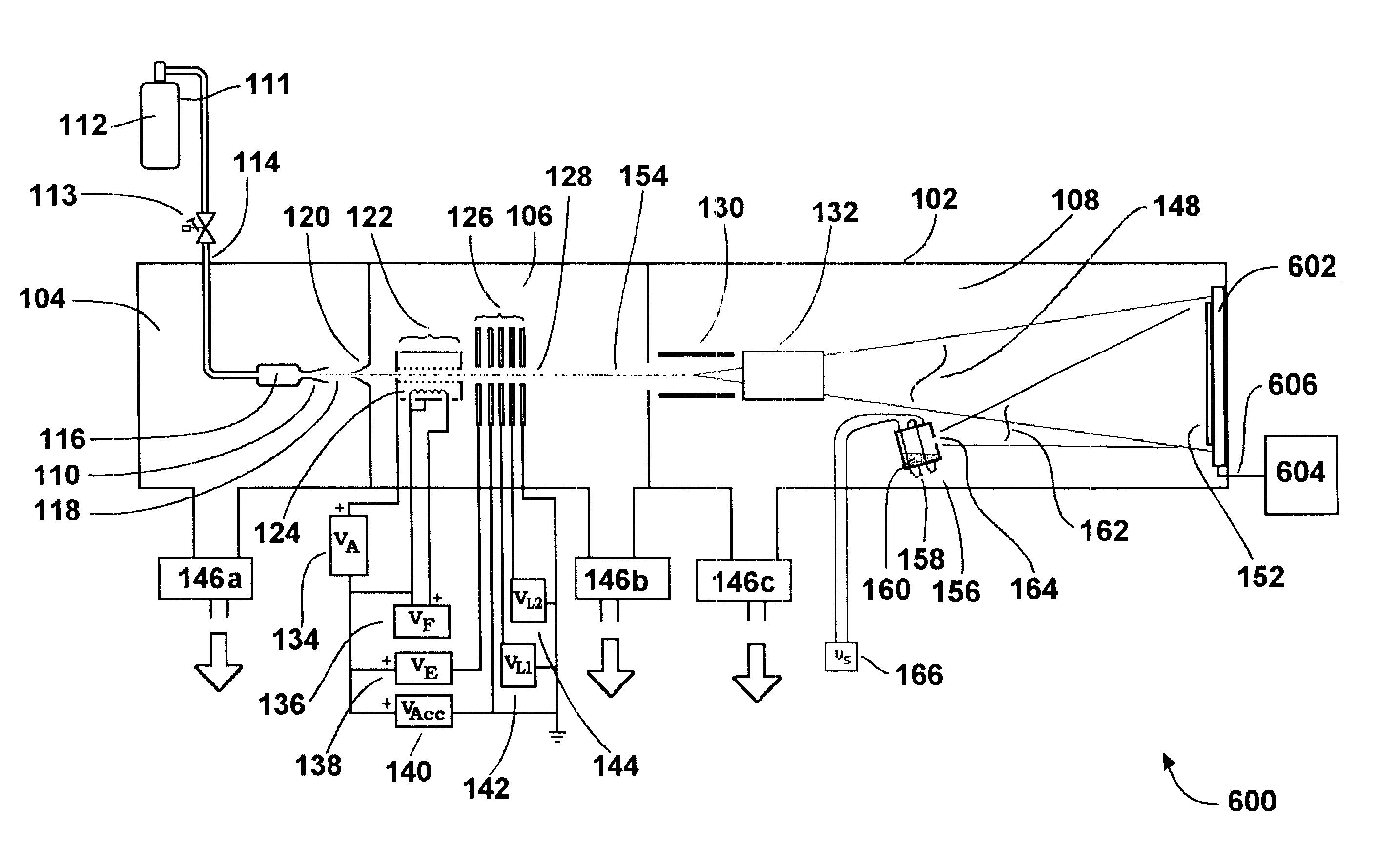
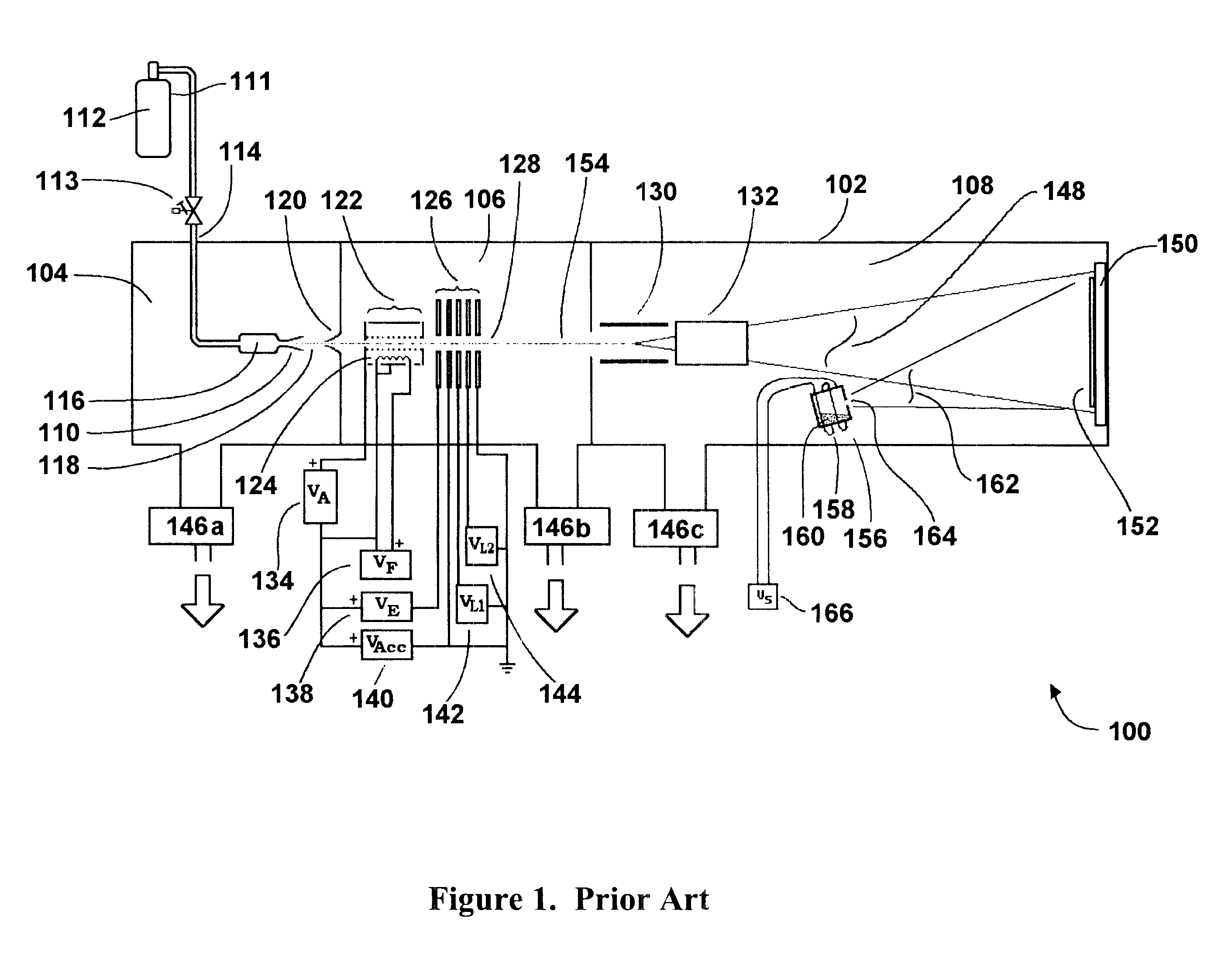
FIG. 1 shows a typical configuration for a GCIB processing system 100 of a form known in prior art, which has capability to perform GCIB processing including GCIB assisted deposition, and which may be described as follows: a vacuum vessel 102 is divided into three communicating chambers, a source chamber 104, an ionization / acceleration chamber 106, and a processing chamber 108,. The three chambers are evacuated to suitable operating pressures by vacuum pumping systems 146a, 146b, and 146c, respectively. A condensable source gas 112 (for example an inert gas such as argon or a reactive gas such as N.sub.2) stored in a cylinder 111 is admitted under pressure through gas metering valve 113 and gas feed tube 114 into stagnation chamber 116 and is ejected into the substantially lower pressure vacuum through a properly shaped nozzle 110. A supersonic gas jet 118 results. Cooling, which results from the expansion in the jet, causes a portion of the gas jet 118 to condense into clusters, ea...


PUM

PropertyMeasurementUnit
Angleaaaaaaaaaa
Angleaaaaaaaaaa
Temperatureaaaaaaaaaa

Abstract

Methods are disclosed for gas-cluster ion-beam deposition of thin films on silicon wafers rendered free of native oxides by termination of the surface bonds and subsequent reactive deposition. Hydrogen termination of the surface of silicon renders it inert to reoxidation from oxygen-containing environmental gasses, even those found as residue in vacuum systems, such as those used to deposit films. Nitrogen termination improves the interface with overlying metal-oxide thin films. The film is formed in intimate contact with the silicon crystal surface forming a nearly ideal interface.

Description

BACKGROUND OF THE INVENTIONThis invention relates generally to the formation of thin films, and, more particularly to the formation of thin dielectric films by gas-cluster ion-beam (GCIB) on surfaces rendered free of native oxides to assure high quality interfacial layers and films.The use of a GCIB for etching, cleaning, and smoothing of the surfaces of various materials is known in the art (See for example, U.S. Pat. No. 5,814,194, Deguchi, et al., "Substrate Surface Treatment Method", 1998). Means for creation of and acceleration of such GCIBs are also described in the Deguchi reference. It is also known (U.S. Pat. No. 5,459,326, Yamada, "Method for Surface Treatment with Extra-Low-Speed Ion Beam", 1995) that atoms in a cluster ion are not individually energetic enough (on the order of a few electron volts) to significantly penetrate a surface to cause the residual sub-surface damage typically associated with the other types of ion beam processing in which individual ions may hav...

Claims


Application Information

Patent Timeline
IPC IPC(8): C23C14/00C23C14/02H01L21/02H01L21/318H01L21/28H01L21/316H01L21/311H01L21/8242H01L21/8246H01L27/105H01L27/108H01L29/51
CPCC23C14/0031C23C14/022H01L21/02054H01L21/0206H01L21/0217H01L21/02172H01L21/02247H01L21/02263H01L21/02299H01L21/02307H01L21/28194H01L21/28202H01L21/28211H01L21/31604H01L21/31662H01L21/31683H01L21/3185H01L28/40H01L29/517H01L29/518H01J2237/0812H01L21/31111H01L29/513
Inventor FENNER, DAVID B.
Owner JDSU OPTICAL
Why Eureka
Try Eureka