SOI transistor with polysilicon seed

a technology of polysilicon seed and transistor, which is applied in the direction of transistors, semiconductor devices, electrical apparatus, etc., can solve the problems of reducing the active device dimension, limiting the performance which can be obtained, and difficulty in scaling semiconductor structures

Inactive Publication Date: 2003-02-18
GLOBALFOUNDRIES US INC
View PDF5 Cites 42 Cited by
  • Summary
  • Abstract
  • Description
  • Claims
  • Application Information

AI Technical Summary

Benefits of technology

It is a further object of the invention to provide a transistor design suitable for extremely high density integration which allows increased precision of location of implanted impurities and precision of geometry of impurity concentration gradients.
It is another object of the invention to provide a manufacturing method which can be carried out with high manufacturing yield to form high performance transistors with much reduced susceptibility to short channel effects.

Problems solved by technology

However, while some structures can be formed at such small sizes, others cannot and adjustments in operating parameters are often required.
In other cases, difficulty in scaling semiconductor structures when seeking to exploit newly developed lithographic capabilities may be the principal limiting factor in the successful reduction of active device dimensions or limit the performance which can be obtained from an active device of a given size at the limit of lithographic resolution.
Some active device structures simply do not scale well to smaller sizes.
This problem led to the development of lightly doped drain structures, now more generally referred to as extension implants since optimal impurity concentrations can be substantial while the dimensions thereof are generally very small.
Also, gate to substrate capacitance has limited performance and led to so-called "halo" implants to increase the impurity concentration gradient in the substrate below the gate structure.
Many state-of-the-art semiconductor structure designs therefore have a heat budget which cannot be exceeded without compromise of the intended electrical properties of the device.
This can be understood from the fact that a scaling of a transistor to smaller dimensions would require increase in the impurity concentration gradient while that increase in concentration gradient may not be possible or available consistent with annealing after an impurity implantation and other device impurity concentration requirements.
However, certain electrical characteristics and device structure designs may be complicated by the placement of the high quality surface layer on an insulator which insulates it from the bulk or handling substrate provided to reduce fragility of the wafer or chip.
In particular, deep structures, contacts and buried elements such dual gate transistor designs that may provide significant performance enhancements may be difficult to form and process windows may be significantly restricted.
At the same time, however, many semiconductor manufacturing processes are very mature and well-developed and, possibly, having tool costs largely amortized.
However, most such designs, to date, when scaled to extremely small sizes remain subject to a significant degree of short channel effects and / or require new processes which may be expensive and of uncertain manufacturing yield.
In general, reduction of short channel effects has not been optimal due to the physical constraints and difficulties in developing steep impurity profile gradients regardless of the processes attempted.
However, it has recently been fount that conventional contact geometries cannot be directly applied to some technologies or present problems of high current density at some locations within them that are significant to overall device performance.
For example, raised source and drain (RSD) structures must be formed when field effect transistors are formed on very thin SOI in order to provide sufficient volume of silicon to develop silicide contacts (and for other reasons) but these structures and other "flat" structures formed substantially parallel to the substrate surface necessarily have geometries which cannot avoid concentration of current at some location within them.

Method used


Image

  • SOI transistor with polysilicon seed
  • SOI transistor with polysilicon seed
  • SOI transistor with polysilicon seed

Examples


Embodiment Construction

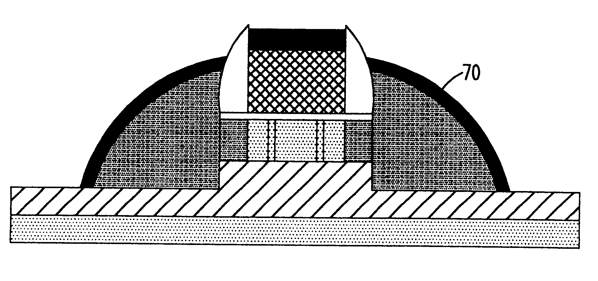
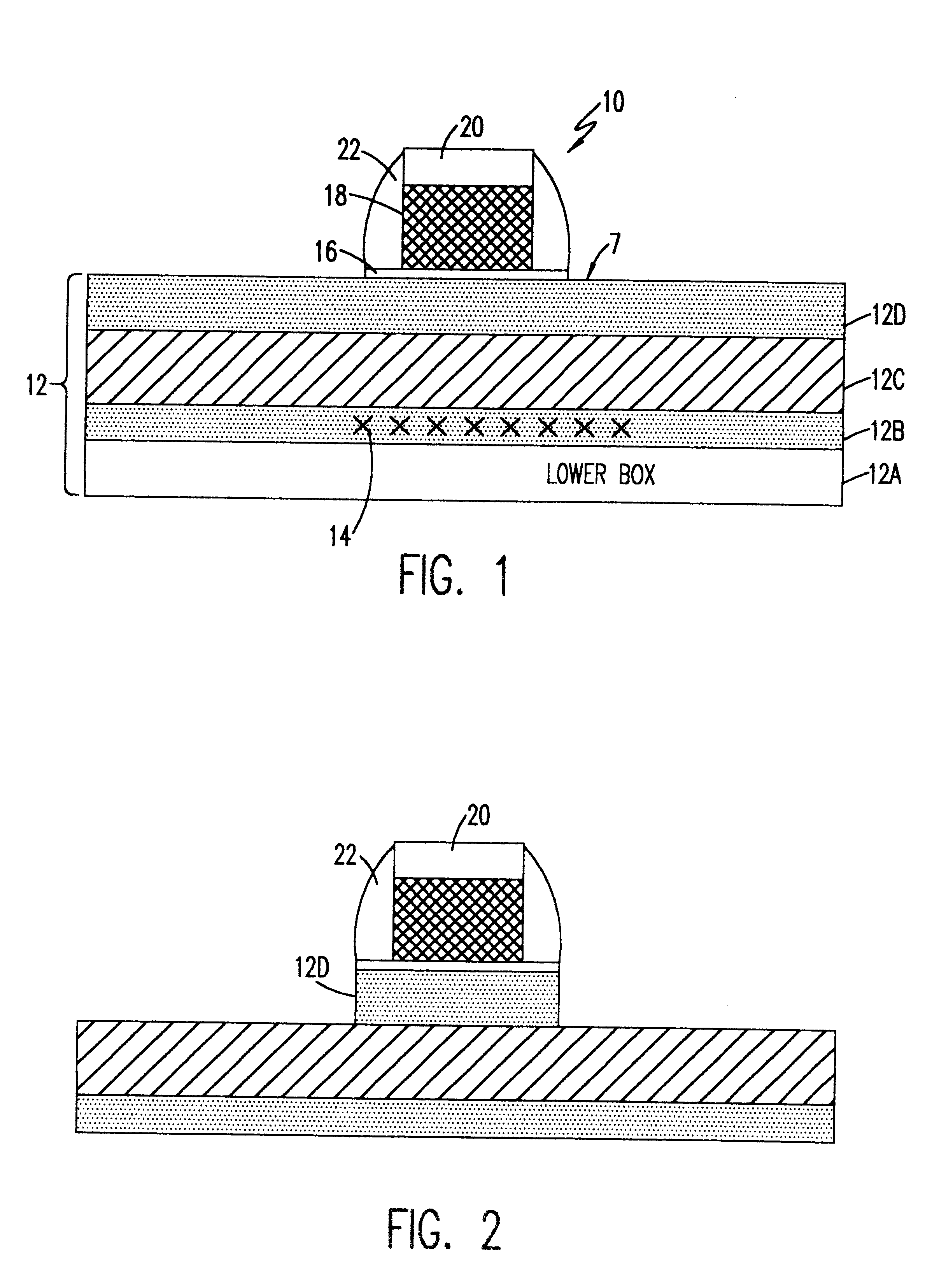
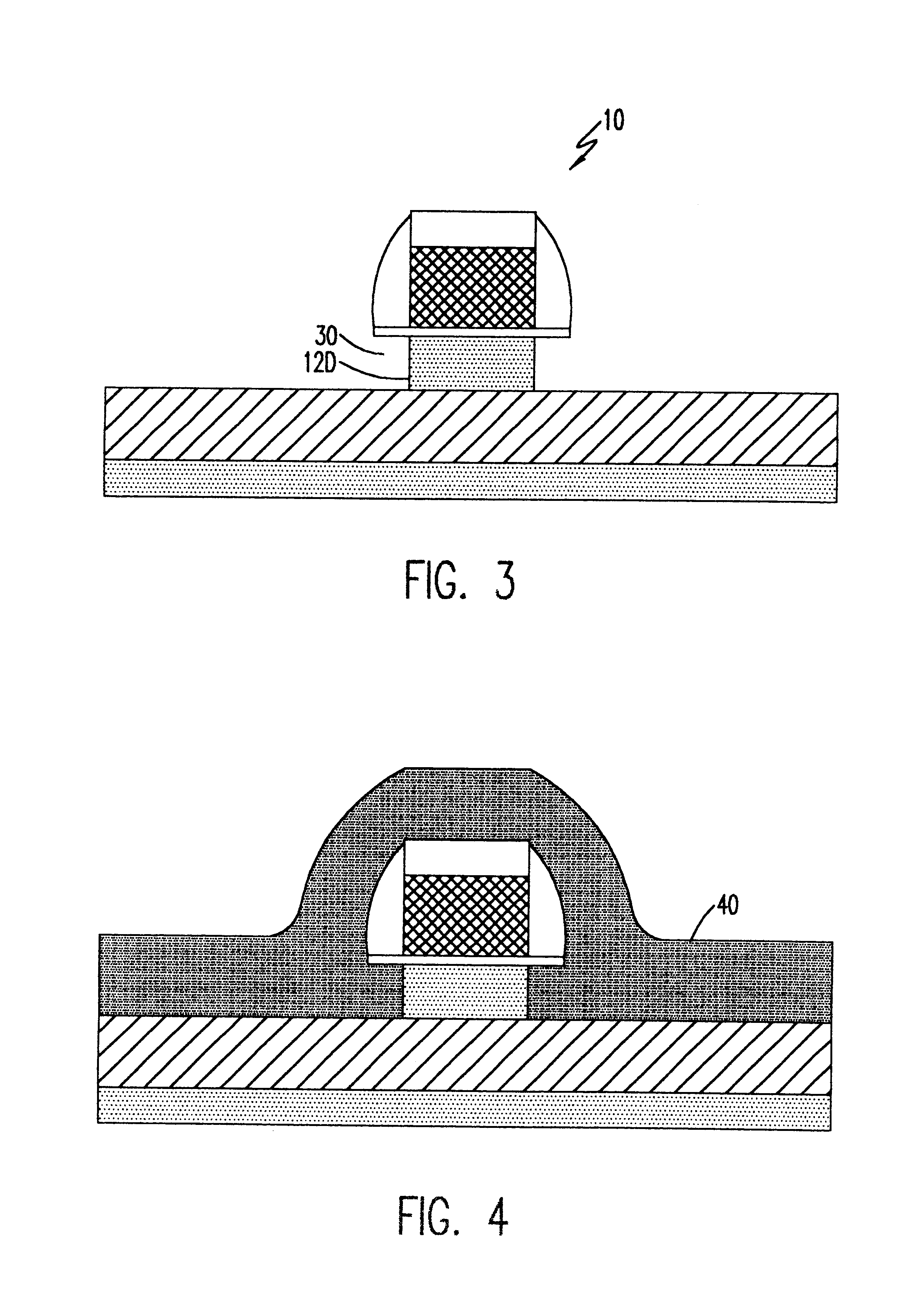
Referring now to the drawings, and more particularly to FIG. 1, there is shown, in cross-section, an early stage in the manufacture of a transistor in accordance with the present invention. Those skilled in the art will recognize that the gate structure 10 is, at this point, similar to conventional gate structures and that the chip or wafer 12 is depicted as a silicon-on-insulator (SOI) structure. It should be appreciated, however, that the invention is also applicable to bulk semiconductor wafers and to semiconductor materials other than silicon and mixtures and alloys thereof, such as SiGe on insulator. The configuration of the various layers of the SOI is not at all critical to the practice of the invention and is depicted principally for illustrative purposes to demonstrate compatibility of the invention with virtually any such configuration. By the same token, a transistor in accordance with the invention can be formed at any location where a layer of silicon overlies a layer o...


PUM


Abstract

Short channel effects are effectively suppressed by steep impurity concentration gradients which can be placed with improved accuracy of location and geometry while relaxing process tolerances by implanting impurities in a polysilicon seed adjacent a conduction channel of a transistor and diffusing impurities therefrom into the conduction channel. The polysilicon seed also allows the epitaxial growth of polysilicon source / drain contacts therefrom having a configuration which minimizes current density and path length therein while providing further mechanical advantages.

Description

1. Field of the InventionThe present invention generally relates to the formation of high performance transistors with reduced short channel effects at small size on wafers or chips of silicon-on-insulator (SOI) construction.2. Description of the Prior ArtThe potential for increased performance and functionality of integrated circuits by increased proximity of devices has provided a strong incentive to increase integration density to decrease length of signal propagation paths, and increase the number of devices which can be formed on a single chip of a given size. Reduction of signal path length reduces interconnection resistance and capacitance and allows reduction of signal propagation time as well as susceptibility to capacitive or inductive coupling of noise. Such reductions in interconnect capacitance must also be accompanied by reductions in device dimensions both to reduce parasitic capacitances which reduce switching speed and to allow optimal reduction of interconnect leng...

Claims


Application Information

Patent Timeline
Patent Type & Authority Patents(United States)
IPC IPC(8): H01L21/02H01L29/66H01L21/336H01L29/786H01L29/41H01L29/78H01L21/28
CPCH01L29/66757H01L29/66772H01L29/78675H01L29/78651H01L29/78618
Inventor ASSADERAGHI, FARIBORZCHEN, TZE-CHIANGMULLER, K. PAULNOWAK, EDWARD J.SHAHIDI, GHAVAM G.
Owner GLOBALFOUNDRIES US INC
Why Eureka
Try Eureka