Semiconductor light emitting device in which near-edge portion is filled with doped regrowth layer, and dopant to regrowth layer is diffused into near-edge region of active layer

a technology of regrowth layer and light-emitting device, which is applied in the direction of solid-state device, laser, semiconductor laser, etc., can solve the problems of so-called catastrophic optical mirror damage (comd), damage to end facet, and formation of vicious cycl

Inactive Publication Date: 2003-04-01
NICHIA CORP +1
View PDF13 Cites 10 Cited by
  • Summary
  • Abstract
  • Description
  • Claims
  • Application Information

AI Technical Summary

Benefits of technology

Another object of the present invention is to provide a process which can produce a semiconductor light emitting device being reliable in a high output power operation, through a small number of manufacturing steps with high reproducibility.
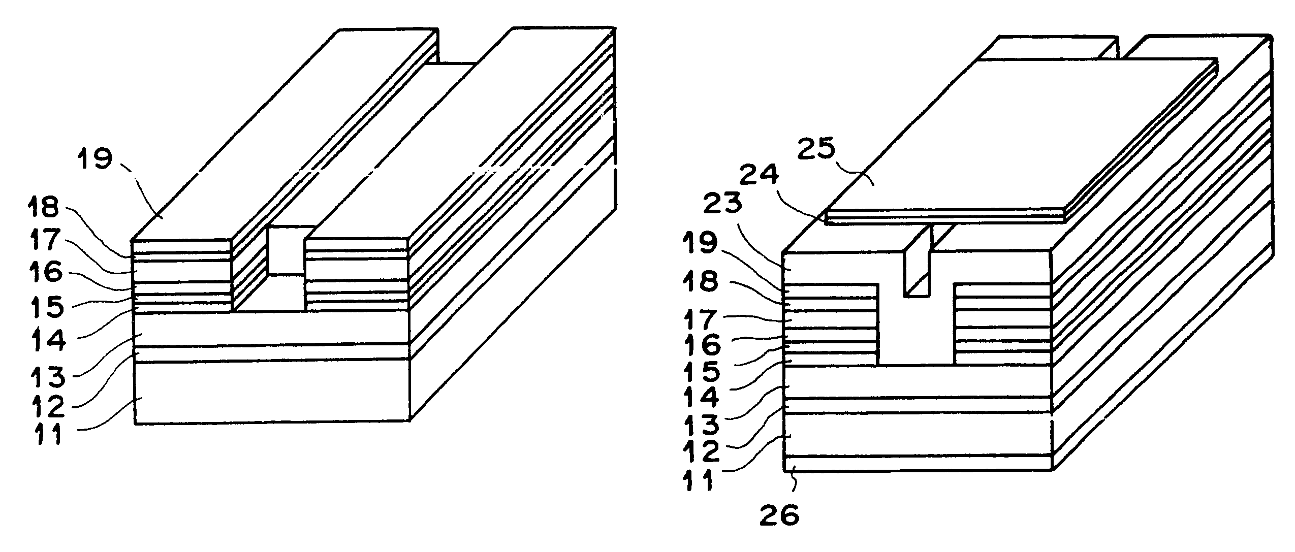
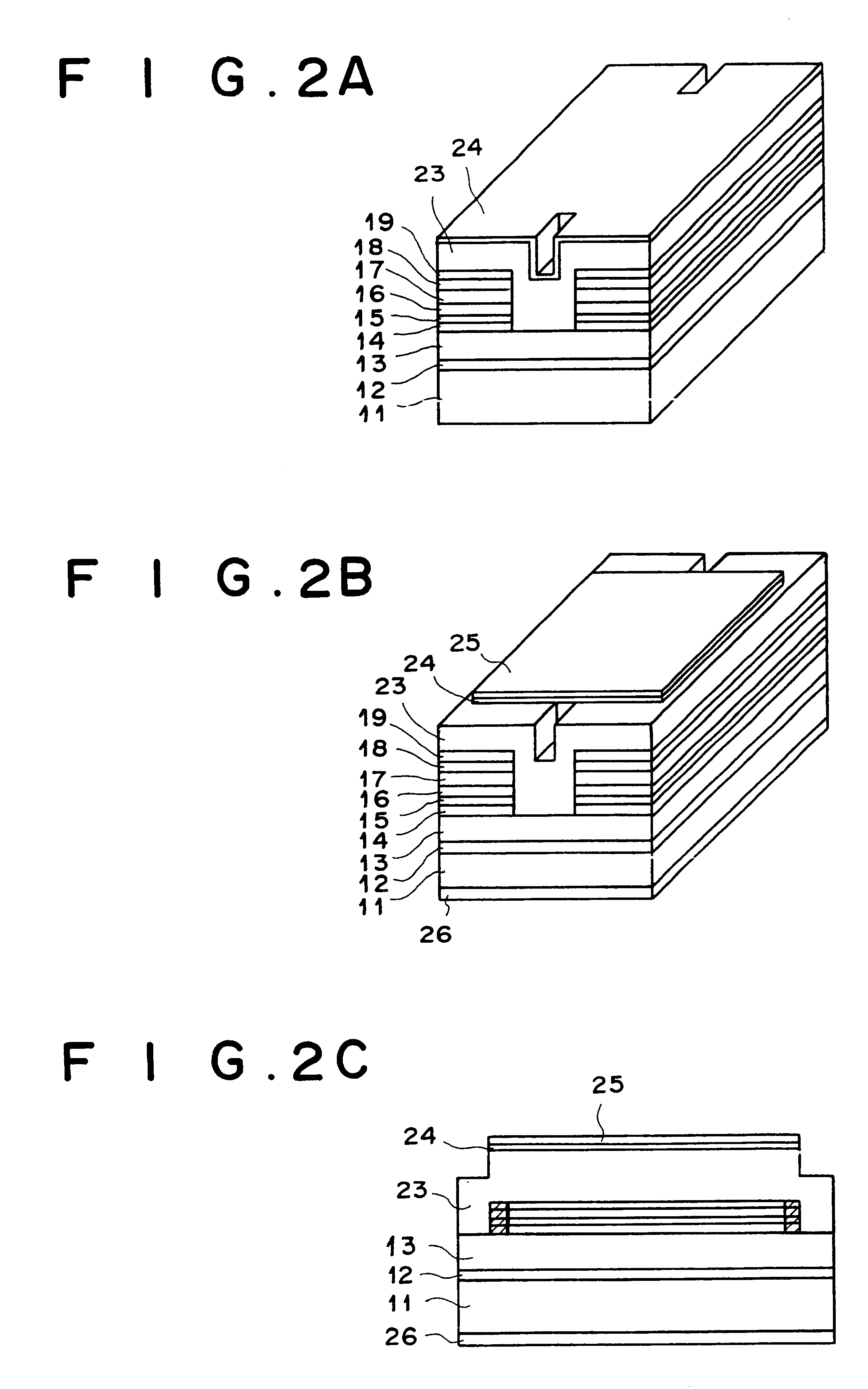
In the semiconductor light emitting device according to the first aspect of the present invention, at least one space is produced between at least one end facet and the at least one near-edge region of the active zone, and is filled with the regrowth layer so that the dopant with which the regrowth layer is doped is diffused into the at least one near-edge region of the active layer. Therefore, crystal mixture occurs in the at least one near-edge region of the active layer, and the energy gap in the at least one near-edge region of the active layer is increased. Thus, the light absorption in the at least one near-edge region of the active layer is reduced. In particular, even when the output power is increased, and the temperature rises, the light absorption in the at least one near-edge region of the active layer can be reduced. Therefore, it is possible to obtain a semiconductor light emitting device which is reliable even in a high output power operation.
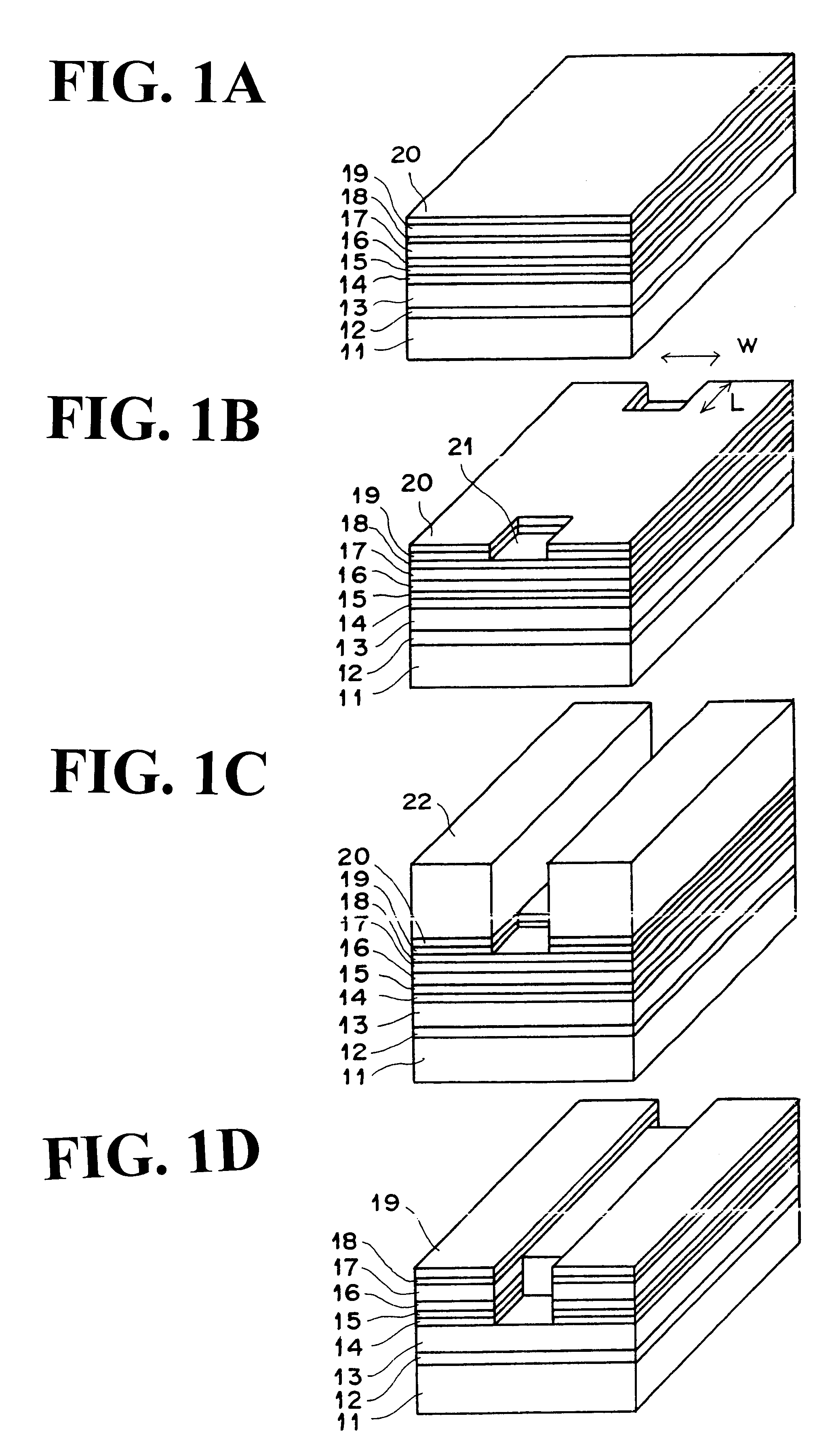
When the semiconductor light emitting device according to the first aspect of the present invention has the above additional feature (i), and the at least one space between the at least one end facet and the at least one near-edge region of the active layer is produced by forming a lamination of the lower cladding layer, the active zone, the upper cladding layer, and the current confinement layer on the substrate, and etching off at least one near-edge portion of the lamination having a depth corresponding to the bottom of the active layer or a lower elevation, and the groove is produced by etching off a stripe portion of the lamination being located inside the at least one space and having the depth corresponding to the bottom of the current confinement layer or a lower elevation, the etching-off operations for producing the at least one space and the groove can be performed concurrently by an identical lithography process or a self alignment process. Therefore, the number of manufacturing steps can be reduced.
(iv) The second conductive type is a p type, to and the dopant is Zn. In this case, the bandgap in the vicinity of the end facet can be satisfactorily increased. Therefore, the light absorption in the vicinity of the end facet can be reduced, and high reliability can be maintained even in a high output power operation.
In addition, since the at least one near-edge space for the end-facet window structure and the groove for the internal stripe structure are formed by one lithography process, the at least one near-edge space produced by the removal of the at least one near-edge portion is well aligned with the stripe groove without any provision for realizing the alignment, and the reproducibility in the formation of the end-facet window structure and the groove for the internal stripe structure is high.
Further, since the near-edge portion of the active zone is removed, and is thereafter filled with the regrowth layer, the dopant of the second conductive type in the regrowth layer can be diffused into the at least one near-edge portion of the active layer with high reliability and reproducibility during the formation of the regrowth layer.

Problems solved by technology

That is, a vicious cycle is formed, and the end facet is damaged.
This damage is the so-called catastrophic optical mirror damage (COMD).
Thus, the maximum optical output power is limited due to the COMD.
Since, in the above process, the dopant is diffused into the quantum-well active layer through the cladding layer and an optical waveguide layer during the formation of the regrowth layer, the diffusion depth of the dopant and the degree of the crystal mixture vary due to irregularity of thermal diffusion occurring during the formation of the regrowth layer, and therefore the window structure has poor reproducibility.
Thus, it is difficult to produce, at a high yield rate, the above semiconductor laser device so that the semiconductor laser device is reliable in a high output power operation.
That is, the manufacturing process is complicated, and the manufacturing cost is high.

Method used


Image

  • Semiconductor light emitting device in which near-edge portion is filled with doped regrowth layer, and dopant to regrowth layer is diffused into near-edge region of active layer
  • Semiconductor light emitting device in which near-edge portion is filled with doped regrowth layer, and dopant to regrowth layer is diffused into near-edge region of active layer
  • Semiconductor light emitting device in which near-edge portion is filled with doped regrowth layer, and dopant to regrowth layer is diffused into near-edge region of active layer

Examples


first example

of Use

A first example of use of the semiconductor laser device as the above embodiment is explained below with reference to FIG. 4, which is a diagram illustrating an outline of a construction of a solid-state laser apparatus which generates a second harmonic. In the example of FIG. 4, the semiconductor laser device as the above embodiment is used as an excitation light source in the solid-state laser apparatus.

The solid-state laser apparatus of FIG. 4 comprises a semiconductor laser device 71, a lens 72, a solid-state laser crystal 73, an output mirror 74, a KNbO.sub.3 nonlinear crystal 75, a coating film 76, a beam splitter 77, and a light receiving element 78. The semiconductor laser device 71 is the semiconductor laser device as the embodiment of the present invention, and emits single-mode light as the excitation light. The lens 72 collects the excitation light emitted from the semiconductor laser device 71. The solid-state laser crystal 73 is excited by the collected excitatio...

second example

of Use

A second example of use of the semiconductor laser device as the embodiment is explained below with reference to FIG. 5, which is a diagram illustrating an outline of a construction of another solid-state laser apparatus which generates a second harmonic. In the example of FIG. 5, the semiconductor laser device as the above embodiment is also used as an excitation light source in the solid-state laser apparatus.

The laser apparatus of FIG. 5 comprises a Peltier element 80, a semiconductor laser device 81, a waveguide grating 82, a MgO-LN waveguide SHG (second harmonic generator) 83, a beam splitter 86, and a light receiving element 87. The semiconductor laser device 81 is the semiconductor laser device as the embodiment of the present invention, and emits single-mode light as the excitation light. The semiconductor laser device 81, the waveguide grating 82, and the MgO-LN waveguide SHG 83 are mounted on the Peltier element 80, and the temperature of the semiconductor laser devi...


PUM


Abstract

In a process for producing a semiconductor light emitting device, first, a lamination including an active zone, cladding layers, and a current confinement layer is formed. Then, a near-edge portion of the lamination having a stripe width is removed so as to produce a first space, and a second near-edge portion located under the first space and a stripe portion of the lamination being located inside the first space and having the stripe width are concurrently removed so that a second space is produced, and cross sections of the active layer and the current confinement layer are exposed in the second space. Finally, the first and second spaces are filled with a regrowth layer so that a dopant to the regrowth layer is diffused into a near-edge region of the remaining portion of the active layer.

Description

1. Field of the InventionThe present invention relates to a semiconductor light emitting device having an end-facet window structure which prevents carrier recombination at a light-exit end facet. The present invention also relates to a process for producing such a semiconductor light emitting device.2. Description of the Related ArtIn conventional semiconductor light emitting devices, when optical output power is increased, currents generated by optical absorption in vicinities of end facets generate heat, i.e., raise the temperature at the end facets. In addition, the raised temperature reduces the semiconductor bandgaps at the end facets, and therefore the optical absorption is further enhanced. That is, a vicious cycle is formed, and the end facet is damaged. This damage is the so-called catastrophic optical mirror damage (COMD). Thus, the maximum optical output power is limited due to the COMD. In order to overcome the above problem, various techniques have been proposed for th...

Claims


Application Information

Patent Timeline
Patent Type & Authority Patents(United States)
IPC IPC(8): H01S5/00H01S5/16H01S5/30H01L33/00H01L33/14H01S5/223H01S5/343
CPCH01S5/164H01L33/145H01S5/305
Inventor KUNIYASU, TOSHIAKI
Owner NICHIA CORP
Why Eureka
Try Eureka