

Composite material used in making printed wiring boards
a technology of composite materials and printed wiring boards, which is applied in the direction of insulating substrate metal adhesion improvement, conductive pattern formation, transportation and packaging, etc. it can solve the problems of difficult to handle an extremely thin metal foil, sometimes occurring tears or wrinkles, and adding complexity to the process of making via holes. , to achieve the effect of accurately etching and reducing the thickness of the conductive material
- Summary
- Abstract
- Description
- Claims
- Application Information
AI Technical Summary
Benefits of technology
Problems solved by technology
Method used
Image

Examples
example 1
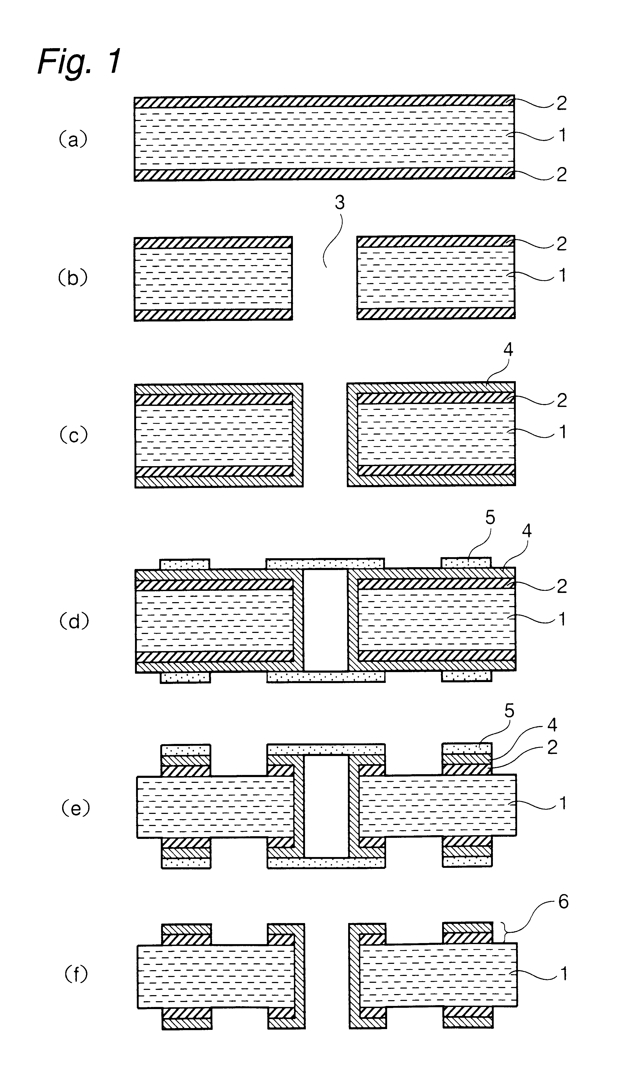
Preparation of Composite Material
An electrolytic copper foil having a thickness of 35 .mu.m was prepared as a metal foil carrier. The shiny side surface of the electrolytic copper foil was cleaned for 30 seconds in a cleaning liquid containing sulfuric acid in a concentration of 100 g / L. After the sulfuric acid cleaning, the copper foil was rinsed with purified water.
Then, the copper foil was immersed in an aqueous solution of ammonium sulfide having a concentration 10 g / L at 30.degree. C. for 10 seconds to form a release layer of copper sulfide on the shiny side surface of the copper foil. The release layer of copper sulfide was rinsed with purified water for 10 seconds, and the copper foil with the release layer was electroplated for 5 seconds at a current density of 20 A / dm.sup.2 using a plating bath containing 20 g / L of copper and 70 g / L of sulfuric acid at a bath temperature of 40.degree. C., to deposit conductive fine particles of copper on the surface of the release layer.
The...
example 2
An electrolytic copper foil having a thickness of 35 .mu.m was prepared as a metal foil carrier. The shiny side surface of the electrolytic copper foil was cleaned for 30 seconds in a cleaning liquid containing sulfuric acid in a concentration of 100 g / L. After the sulfuric acid cleaning, the copper foil was rinsed with purified water.
Then, the shiny side surface of the copper foil was immersed in an aqueous solution containing triazinethiol in a concentration of 5 g / L at a liquid temperature of 40.degree. C. for 30 seconds to form an organic release layer on the copper foil carrier surface. Then, the surface of the organic release layer was rinsed. The copper foil with the organic release layer was electroplated at a current density of 15 A / dm.sup.2 using a plating bath containing 10 g / L of copper and 170 g / L of sulfuric acid with a bath temperature of 30.degree. C. to deposit conductive fine particles.
The resulting composite foil having the conductive fine particles thereon was el...
example 3
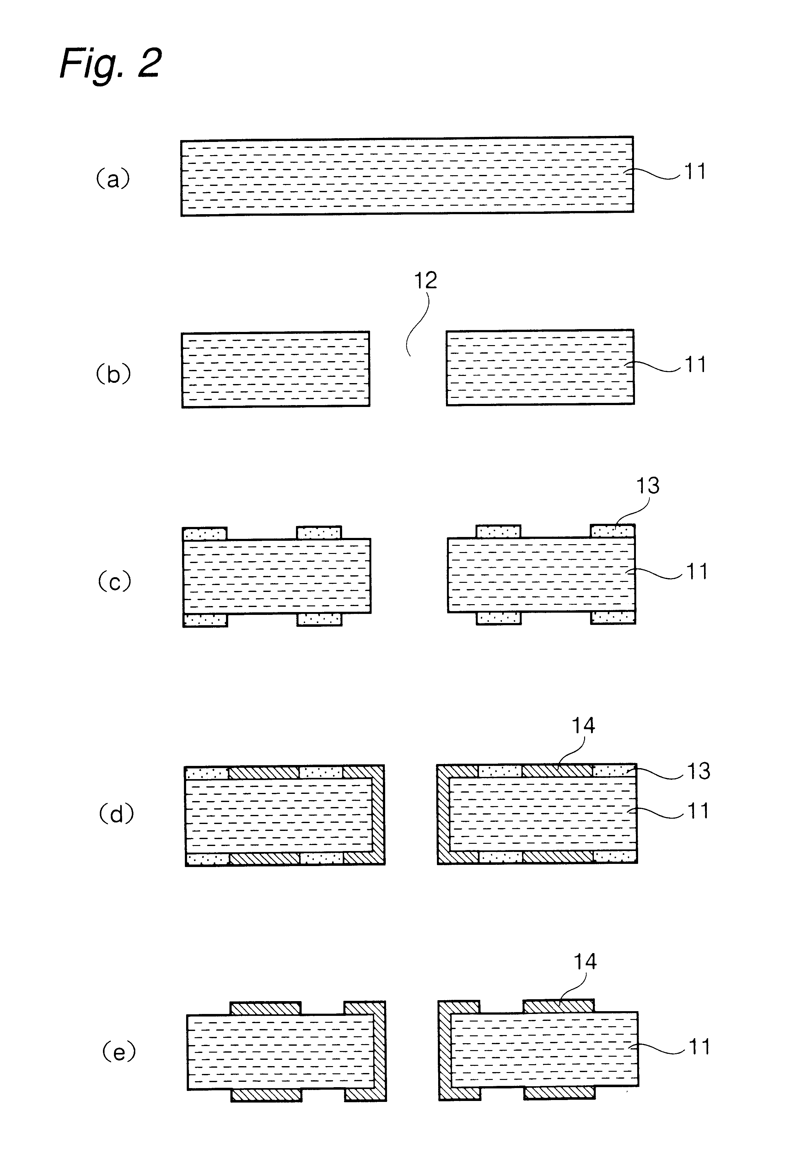
Preparation of Composite Material
An aluminum alloy foil (Al--Mn alloy foil) having a thickness of 40 .mu.m is prepared as a metal foil carrier. The aluminum alloy foil is immersed in a plating bath at pH 8.5 containing 30 g / L of sodium hydroxide, 40 g / L of sodium carbonate and 35 g / L of Rochelle salt at a bath temperature of 30.degree. C. for 30 seconds to perform electroless plating of zinc. After forming the plated layer of zinc, the aluminum alloy foil is rinsed with purified water for 30 seconds.
Then, the aluminum alloy copper foil with the zinc plated layer is electroplated for 5 seconds at a current density of 7 A / dm.sup.2 using a plating bath at pH 9 containing 20 g / L of copper and 70 g / L of potassium diphosphate at a bath temperature of 25.degree. C., to deposit conductive fine particles of copper on the surface of the zinc plated layer.
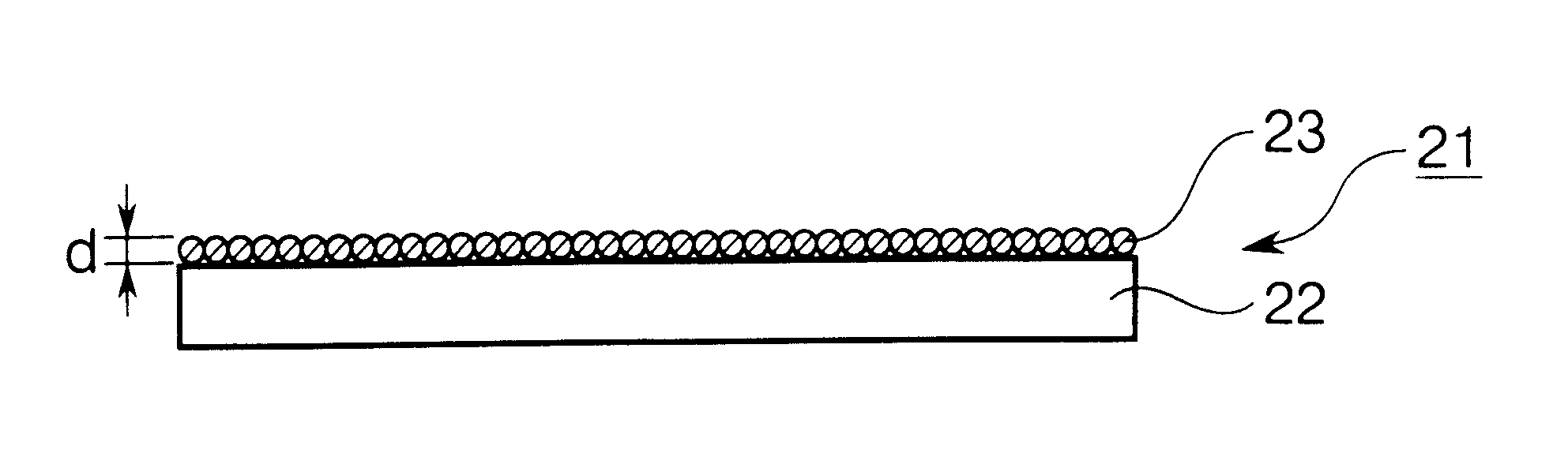
The dimension of the conductive fine particles is 0.1 .mu.m in the direction of the composite material.
Then, the composite material obtained...
PUM
| Property | Measurement | Unit |
|---|---|---|
| thickness | aaaaa | aaaaa |
| thickness | aaaaa | aaaaa |
| current density | aaaaa | aaaaa |
Abstract
Description
Claims
Application Information