Solar cells using fullerenes

a fullerene, solar cell technology, applied in the field of solar cells, can solve the problems of high cost, large surface area of efficient crystalline-based devices, difficult and expensive production, etc., and achieve the effect of great improvement efficiency

Inactive Publication Date: 2003-06-17
THE TRUSTEES FOR PRINCETON UNIV
View PDF15 Cites 493 Cited by
  • Summary
  • Abstract
  • Description
  • Claims
  • Application Information

AI Technical Summary

Benefits of technology

The present invention provides organic-based solar cells with greatly improved efficiency. These PV devices comprise an anode layer, an organic hole transporting (donor-type) layer, an electron transporting (acceptor-type) layer comprising a fullerene, and a cathode. Advantageously, the device also includes one or more exciton blocking layers (EBL) between the ETL and the cathode and / or between the anode and the HTL.
On the other hand, another countervailing consideration is that as the separation between the exciton dissociating interface and the adjacent electrodes increases, the electric field region around the interface will have a higher value over a greater volume. As light absorption increases with increasing electric field strength, more excitons will be generated. Also, the higher electric fields will also promote faster exciton dissociation.

Problems solved by technology

However, efficient crystalline-based devices, especially of large surface area, are difficult and expensive to produce due to the problems inherent in producing large crystals without significant efficiency-degrading defects.
On the other hand, high efficiency amorphous silicon devices still suffer from problems with stability.
Either of these outcomes is undesirable in a photosensitive optoelectronic device.
The result is that device configuration predictions from donor / acceptor criteria may not be borne out by actual device performance.
However, organic PV devices typically have relatively low quantum yield (the ratio of photons absorbed to carrier pairs generated, or electromagnetic radiation to electricity conversion efficiency), being on the order of 1% or less.
.), requiring a trade off between using a thick, and therefore resistive, cell with multiple or highly folded interfaces, or a thin cell with a low optical absorption efficiency.
To date none of these proposals has led to a significant improvement in overall cell performance, particularly at high illumination intensities.

Method used


Image

  • Solar cells using fullerenes
  • Solar cells using fullerenes
  • Solar cells using fullerenes

Examples


Embodiment Construction

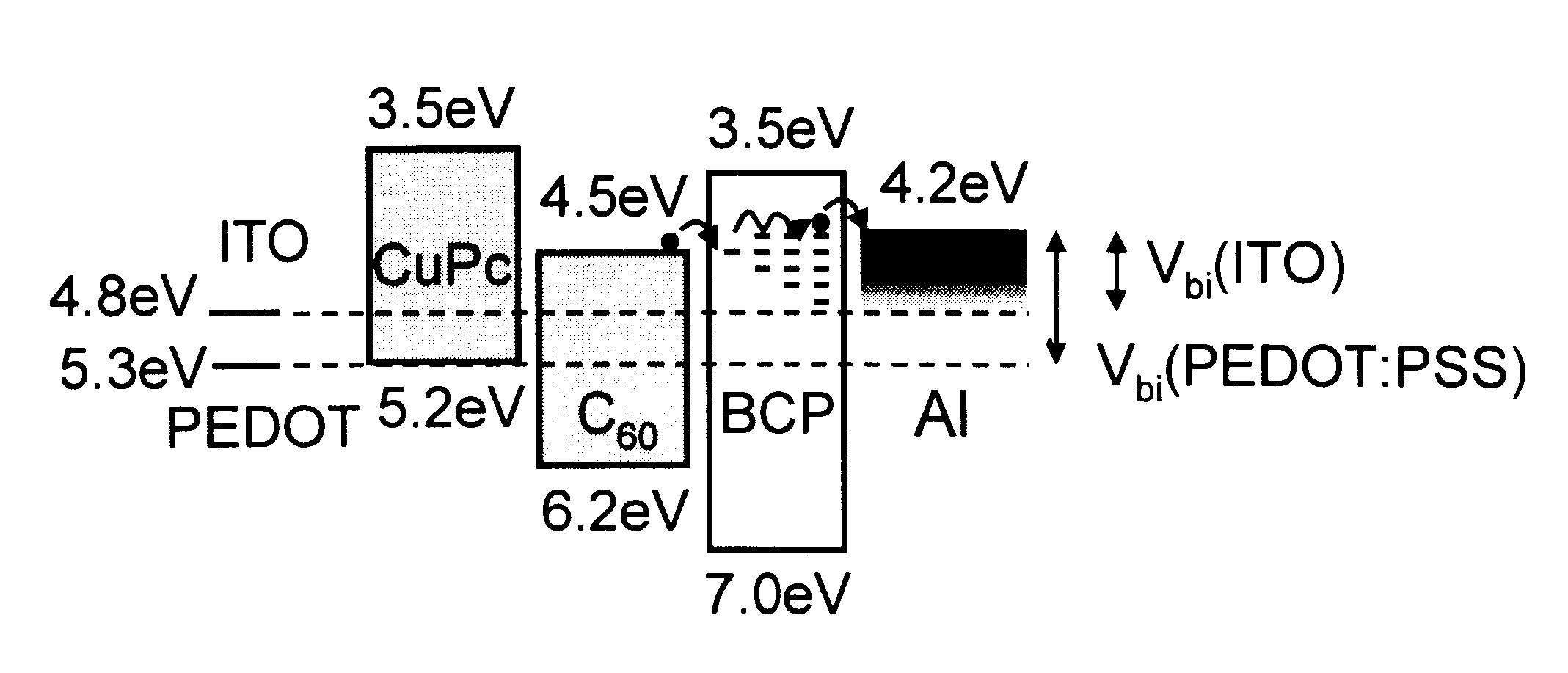
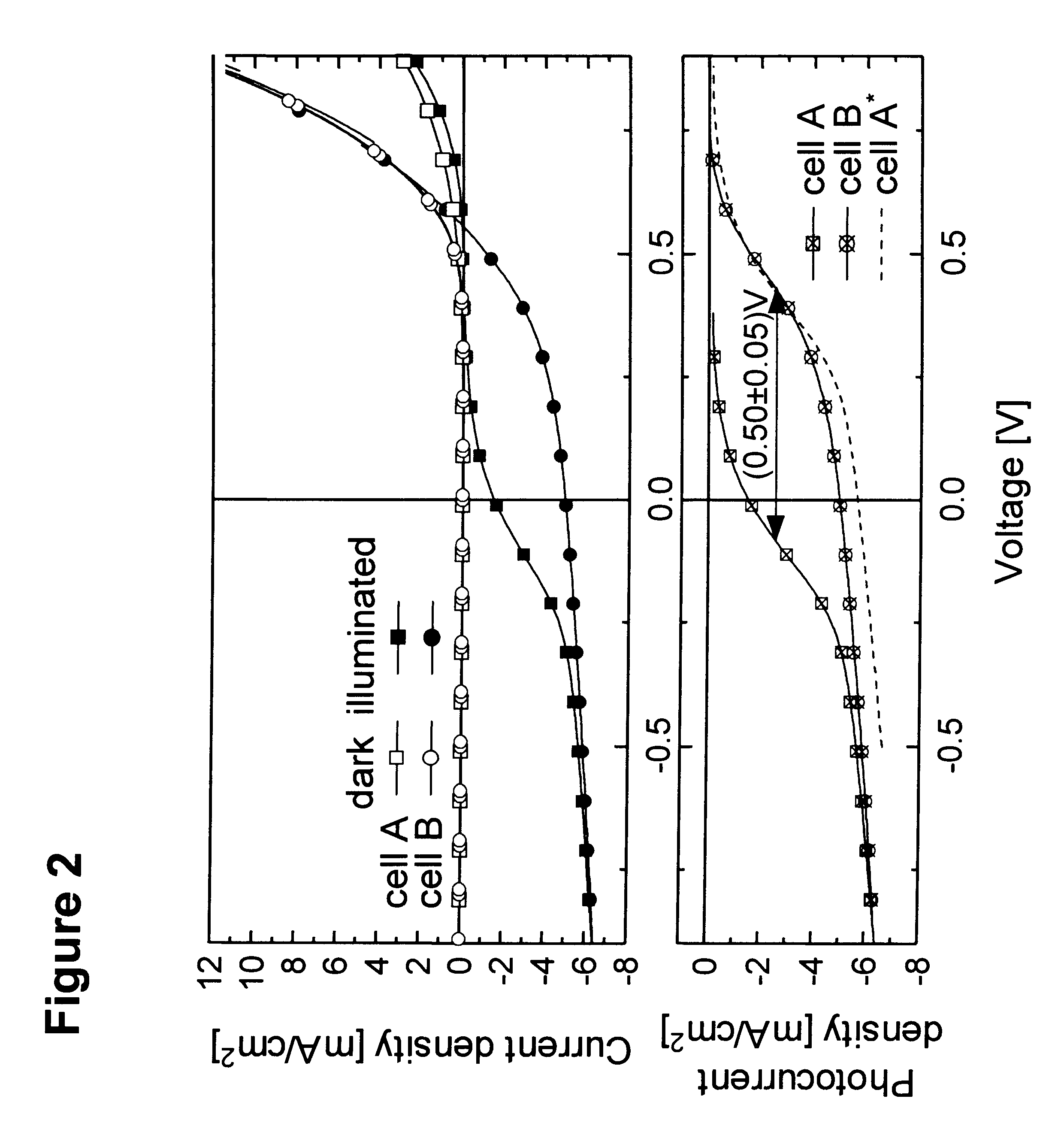
Exemplary embodiments are fabricated on pre-cleaned glass substrates coated with a .about.1400 .ANG. thick transparent, conducting indium-tin-oxide (ITO) anode (with a sheet resistance of 40 .OMEGA. / sq.). After solvent cleaning, the substrates are treated with an O.sub.2 -plasma (50W, 100 mTorr, 5 minutes). Unless otherwise specified, the ITO film is then coated with a (320.+-.10) .ANG. thick film of PEDOT:PSS by spin coating from solution at 4000 rpm for 40 seconds, followed by drying at 90.degree. C. for 15 minutes in vacuum. The organic materials can be obtained commercially, and then purified using thermal gradient sublimation. Films are grown at room temperature in high vacuum (.about.1.times.10.sup.-6 Torr) in the following sequence: a 50 .ANG. to 400 .ANG. thick film of the donor-like copper phthalocyanine (CuPc), followed by a 100 .ANG. to 400 .ANG. thick film of the acceptor-like C.sub.60. Next, a 50 .ANG. to 400 .ANG. thick bathocuproine (BCP) EBL is deposited. The cathode...


PUM

PropertyMeasurementUnit
semi-transparentaaaaaaaaaa
LUMO-HOMOaaaaaaaaaa
thickaaaaaaaaaa

Abstract

Organic photosensitive optoelectronic devices are disclosed. The devises comprise photoconductive organic thin films in a heterostructure, which include an exciton blocking layer to enhance device efficiency. The use of fullerenes in the electron conducting layer has lead to devices with high efficiency. Single heterostructure, stacked and wave-guide type embodiments are disclosed. Devices having multilayer structures and an exciton blocking layer are also disclosed. Guidelines for selection of exciton blocking layers are provided.

Description

The present invention generally relates to organic photosensitive optoelectronic devices. More specifically, it is directed to organic photovoltaic devices, e.g., organic solar cells.Optoelectronic devices rely on the optical and electronic properties of materials to either produce or detect electromagnetic radiation or to generate electricity from ambient electromagnetic radiation. Photosensitive optoelectronic devices convert electromagnetic radiation into electricity. Solar cells, also known as photovoltaic (PV) devices, are used to generate electrical power from ambient light. PV devices are used to drive power consuming loads to provide, for example, lighting, heating, or to operate electronic equipment such as computers or remote monitoring or communications equipment. These power generation applications often involve the charging of batteries or other energy storage devices so that equipment operation may continue when direct illumination from the sun or other ambient light s...

Claims


Application Information

Patent Timeline
Patent Type & Authority Patents(United States)
IPC IPC(8): H01L27/28H01L27/30H01L31/0256H01L51/30H01L51/05H01L31/00H01L51/00
CPCH01L51/424B82Y10/00H01L27/301H01L31/0256H01L2251/308Y02E10/549H01L51/0046H01L51/0078Y10S977/932Y10S977/948H01L51/0037H10K39/10H10K85/1135H10K85/211H10K85/311H10K30/20H10K2102/103
Inventor FORREST, STEPHEN R.PEUMANS, PETER
Owner THE TRUSTEES FOR PRINCETON UNIV
Why Eureka
Try Eureka