GaN selective growth on SiC substrates by ammonia-source MBE

a technology of ammonia-source and substrate, applied in the direction of single crystal growth, polycrystalline material growth, chemistry apparatus and processes, etc., can solve the problems of compromising the performance of certaln types of devices, preventing many possible device applications, and being generally much harder to achiev

Inactive Publication Date: 2003-07-29
NAT RES COUNCIL OF CANADA
View PDF6 Cites 8 Cited by
  • Summary
  • Abstract
  • Description
  • Claims
  • Application Information

AI Technical Summary

Benefits of technology

The lack of gas diffusion may be offset by enhancing atoms' surface mobility through optimizing ammonia flow rate and / or using certain surfactants during growth.

Problems solved by technology

This, however, has proved to be generally much harder than by vapor-phase-based growth processes such as the MOCVD technique.
Also, MBE has in the past been associated with significant surface roughness, and this can preclude many possible device applications.
However, GaN epilayers prepared by this technique generally show a significant surface roughness associated with the sizes of the columnar structures defined by the density of threading dislocations, and these can compromise the performance of certAlN types of devices.

Method used


Image

  • GaN selective growth on SiC substrates by ammonia-source MBE
  • GaN selective growth on SiC substrates by ammonia-source MBE
  • GaN selective growth on SiC substrates by ammonia-source MBE

Examples


Embodiment Construction

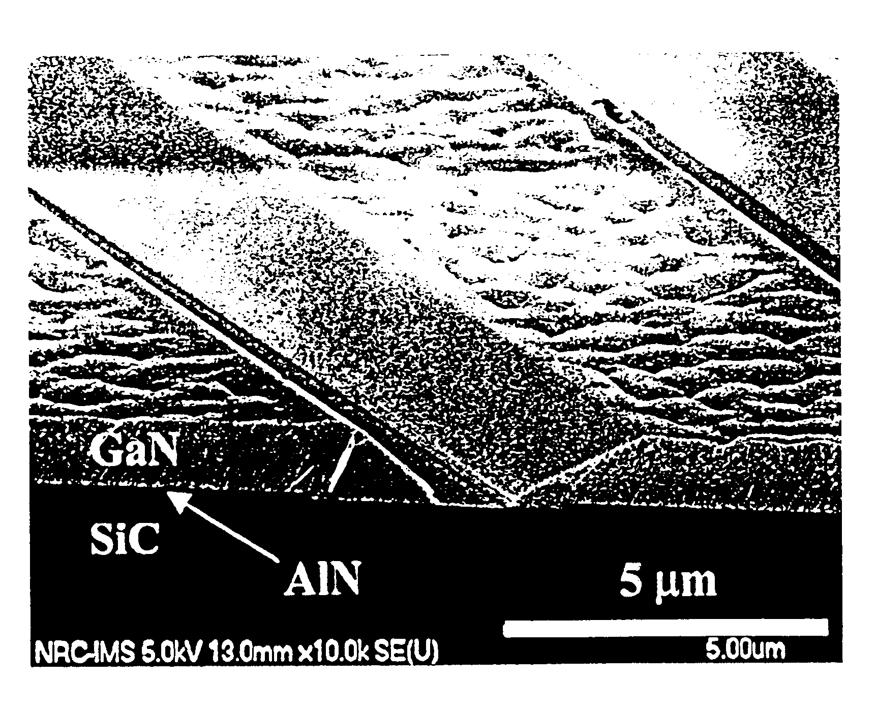
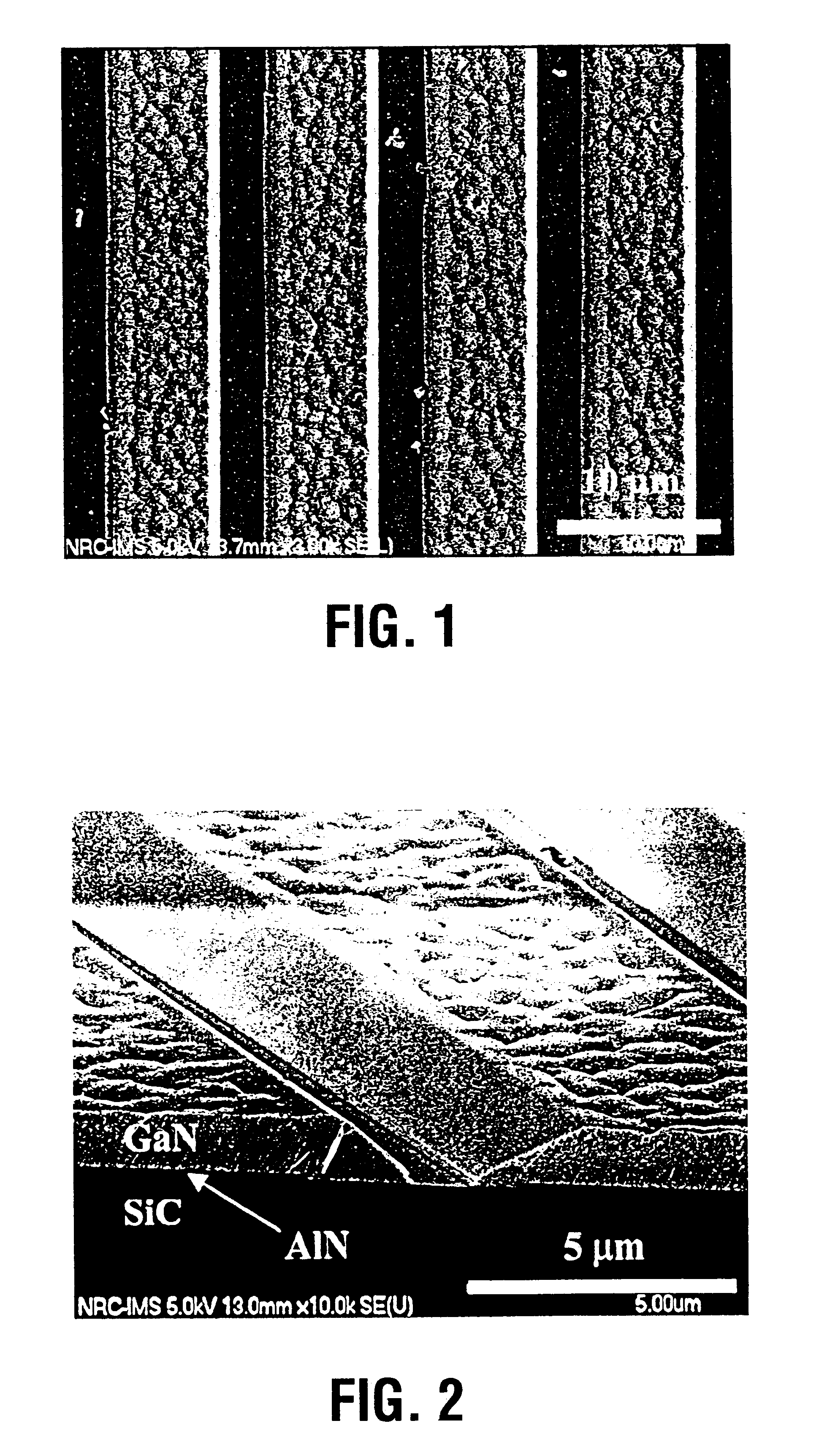
The growth system was a custom-built system operational for both molecular beam epitaxy and magnetron sputter epitaxy using ammonia as the nitrogen source. The magnetron sputter epitaxy technique was used for depositing AlN buffer layers on sapphire or SiC substrates for the subsequent growth of high quality GaN layers by ammonia-MBE. Such a technique is, for example, described in Appl. Phys. Lett 74, 2373 (1999), H. Tang and J. B. Webb, the contents of which are herein incorporated by reference.

The substrate used for the selective growth experiment was a 4H-SiC (0001) wafer with Si-terminated surface. The size of the substrate was a quarter of a 2" wafer. The wafer was back-coated with Mo, degreased with chloroform, dipped in 10% HF for 1 minute, thoroughly rinsed and blown dry with nitrogen. No hydrogen surface treatment was applied. The substrate was mounted indium free on a Mo holder that allows direct radiative heating of the substrate with a graphite heater. The SiC substrate ...


PUM

PropertyMeasurementUnit
thickaaaaaaaaaa
temperatureaaaaaaaaaa
widthaaaaaaaaaa

Abstract

A method is described for selectively depositing a GaN epitaxial layer on a substrate. The substrate is first patterned with a seed layer, preferably of AlN, and then the GaN epitxial layer is grown on the resulting patterned substrate by molecular beam epitaxy (MBE) such that growth occurs selectively over the seed layer.

Description

1. Field of the InventionThis invention relates to the field of molecular beam epitaxy (MBE), and in particular to a method of achieving GaN epitaxial selective growth and lateral overgrowth on a substrate.2. Description of Related ArtGallium nitride epilayers are becoming increasingly important in the manufacture of a number of devices. GaN epilayers are, for example, the crucial technology used for achieving robust CW blue lasers with long lifetime. Selectively grown GaN stripes, prisms and pyramids with their characteristically smooth facets or well defined ridges are ideal candidates for forming optical microcavity, optical waveguides, and InGaN quantum dot structures.The selective growth of GaN has been demonstrated using the metalorganic chemical vapor deposition (MOCVD) technique and successfully used in a variety of applications over the past four or five years. The epitaxial lateral overgrowth enabled by this selective growth process has been shown to bring a dramatic reduc...

Claims


Application Information

Patent Timeline
Patent Type & Authority Patents(United States)
IPC IPC(8): C30B23/02
CPCC30B23/02C30B29/403C30B29/406
Inventor TANG, HAIPENGWEBB, JAMES B.BARDWELL, JENNIFER A.
Owner NAT RES COUNCIL OF CANADA
Why Eureka
Try Eureka