
Control of the deposition temperature to reduce the via and contact resistance of Ti and TiN deposited using ionized PVD techniques

Inactive Publication Date: 2004-01-06
NOVELLUS SYSTEMS
View PDF6 Cites 119 Cited by
  • Summary
  • Abstract
  • Description
  • Claims
  • Application Information

AI Technical Summary

Benefits of technology

It is yet another object of the present invention to provide a method of depositing Ti / TiN liner and barrier layers having decreased processing steps, time and at reduced costs.
Still another object of the present invention is to provide a method of depositing Ti / TiN liner and barrier layers which imparts increased directionality to the atoms reaching the substrate surface.
Another object of the invention is to provide a method of depositing Ti / TiN liner and barrier layers having improved step coverage, grain size, grain orientation and roughness.

Problems solved by technology

This decreases the overall deposition rate of the desired layer of TiN onto the IC substrate because the nitrogen in the titanium target interferes with the sputtering of titanium.
A disadvantage is that the titanium target used to deposit TiN cannot then be used to deposit Ti.
It has been found that TiN deposited in the NNM mode tends to be a poor barrier by itself, often requiring having to anneal the NNM TiN deposited layer, such as by Rapid Thermal Nitridation or Rapid Thermal Anneal, to improve the TiN barrier properties.
However, having to anneal the NNM TiN deposited layer requires additional processing steps and, as such, increases both time and processing expenses.
However, the use of an extra titanium layer has the disadvantage that if a CVD W layer is deposited on the extra Ti layer using WF.sub.6, any free Ti reacts with F to form a layer of TiF.sub.s, to which W has a bad adhesion.
Accordingly, the use of a shutter in the deposition processes of Ti and TiN layers also requires additional processing steps, increases processing time, and increases processing costs.
As the aspect ratio ("AR") of the via increases, i.e., the ratio of the height of the aperture to its width, it has been found that conventional sputtering techniques do not provide acceptable deposition results.
The deposited material at the upper surfaces increasingly accentuates the shadowing effect, thereby prematurely closing the upper section of the via and preventing effective fill of the lower section.
However, collimation techniques are inefficient as much of the target material is wasted and builds up on the cell walls of the filter which can lead to an undesired increase in the number of particulates in the system, making it necessary to replace or clean the collimator frequently.
Also, since most of the sputtered material does not pass through the collimator and is wasted, the deposition rate is slow and the rate of consumption of the target is high.
In such a process, it is necessary to exactly balance and control the sputter power and the flow rates of inert Ar and N.sub.2 gases, however, such control is difficult and the Ti targets often become nitrided.
In either case, a collimator used in either a NM or a NNM mode eventually becomes covered with deposits of Ti and TiN material which tend to flake off the collimator, resulting in contamination of the underlying IC substrate.
Accordingly, it has been recognized that conventional PVD sputtering techniques are inefficient and, in some instances, incapable of providing required directionality to thin films when fabricating VLSI and ULSI circuits.
However, the disadvantages with this method is that the band also gets sputtered, and becomes a consumable.
Additionally, the sputtering of the band can increase the amount of particles created.
By increasing the quantity of collisions, the likelihood increases that a neutral ejected target atom will be struck by a sufficiently energetic particle within the plasma, thus causing the ejected target atom to lose one or more electrons and result in an ionized atom.
However, conventional magnetron and rf-iPVD sputtering techniques are limited in their efficiency as the vast majority of metal atoms ejected from the target remain neutral, i.e., upwards of 98% or greater of the target material atoms remain un-ionized as they travel through the sputter chamber to the substrate.
In particular, when atoms are deposited on substrate surfaces at angles less than normal, it poses significant difficulty in uniformly filling trenches and interconnect vias.
Accordingly, the overall efficiency of such systems are very low as most of the sputtered material remains unionized.
However, many of the IPVD sources suffer from the fact that they cannot produce a sufficiently high density plasma that can adequately ionize the depositing metal species.
This tends to limit the application of medium density plasma IPVD sources (RFIPVD and IMP) for certain applications including that of Ti and TiN liner and barrier layers in semiconductor processing.
Additionally, as the successful management of the thermal budget is critical to a successful implementation of I-PVD, I-PVD for Ti and TiN has not been successfully introduced into semiconductor production due to the temperature control needed for the wafer during ionized deposition.
As such, Ti / TiN liner and barrier depositions for low contact resistance tungsten interconnects continues to be a major challenge for current and future aspect ratios of interconnect vias.
Standard PVD techniques are proven to be inadequate for depositing films in narrow, high aspect ratio structures with necessary and sufficient step coverage as well as the necessary and sufficient via and contact resistance.

Method used


Image

  • Control of the deposition temperature to reduce the via and contact resistance of Ti and TiN deposited using ionized PVD techniques
  • Control of the deposition temperature to reduce the via and contact resistance of Ti and TiN deposited using ionized PVD techniques
  • Control of the deposition temperature to reduce the via and contact resistance of Ti and TiN deposited using ionized PVD techniques

Examples


Embodiment Construction

)

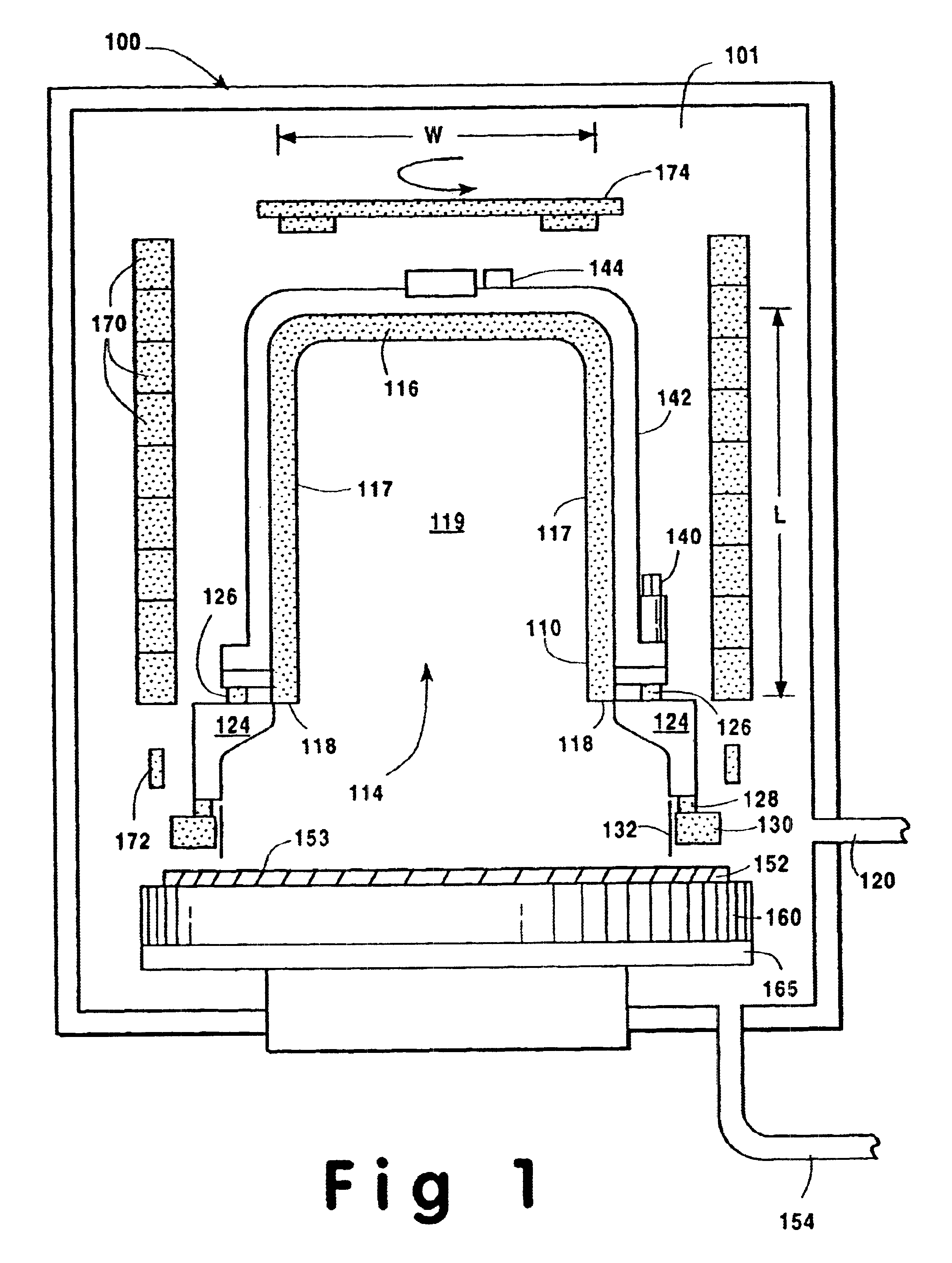
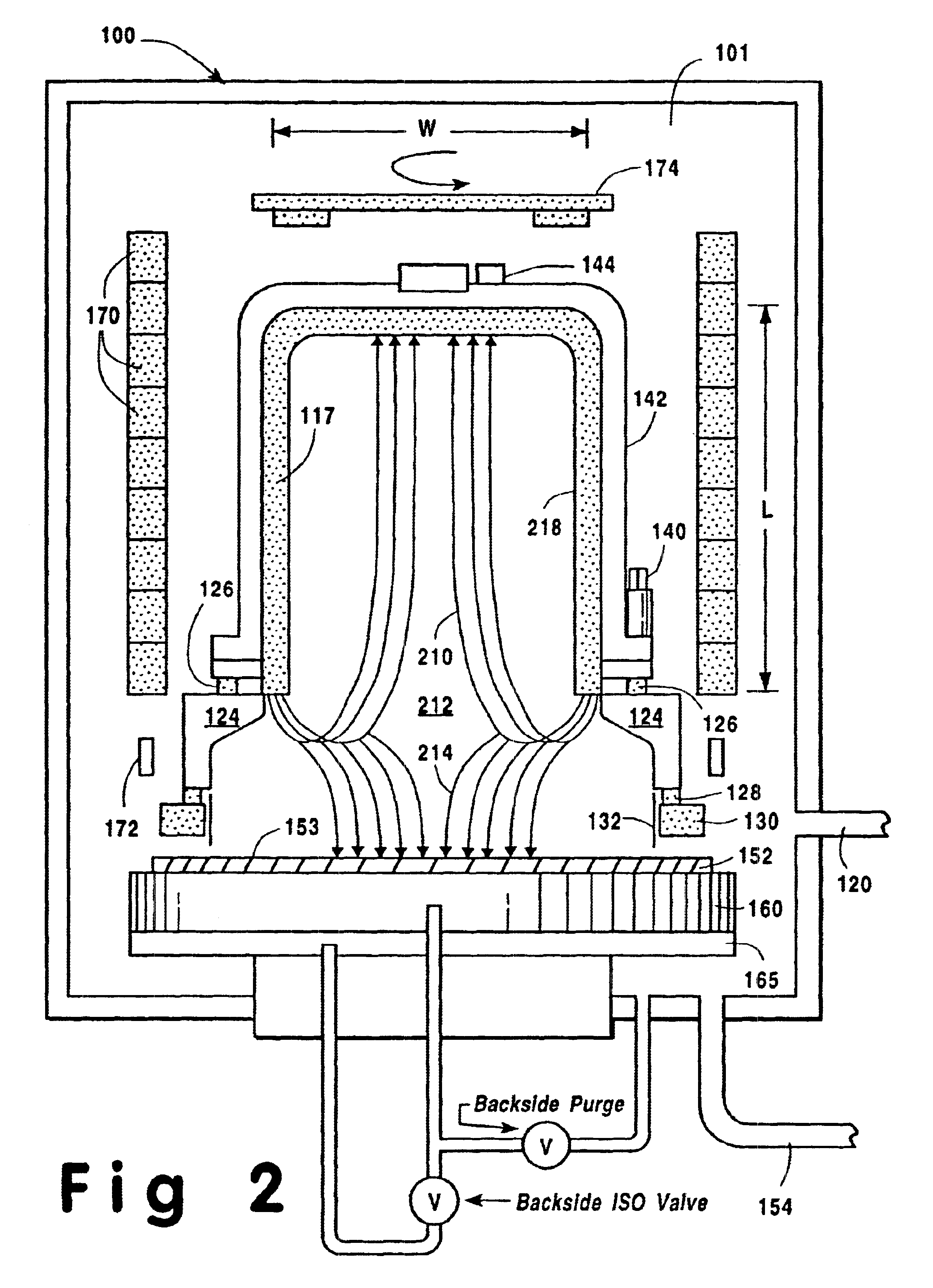
In describing the preferred embodiment of the present invention, reference will be made herein to FIGS. 1-6 of the drawings in which like numerals refer to like features of the invention.

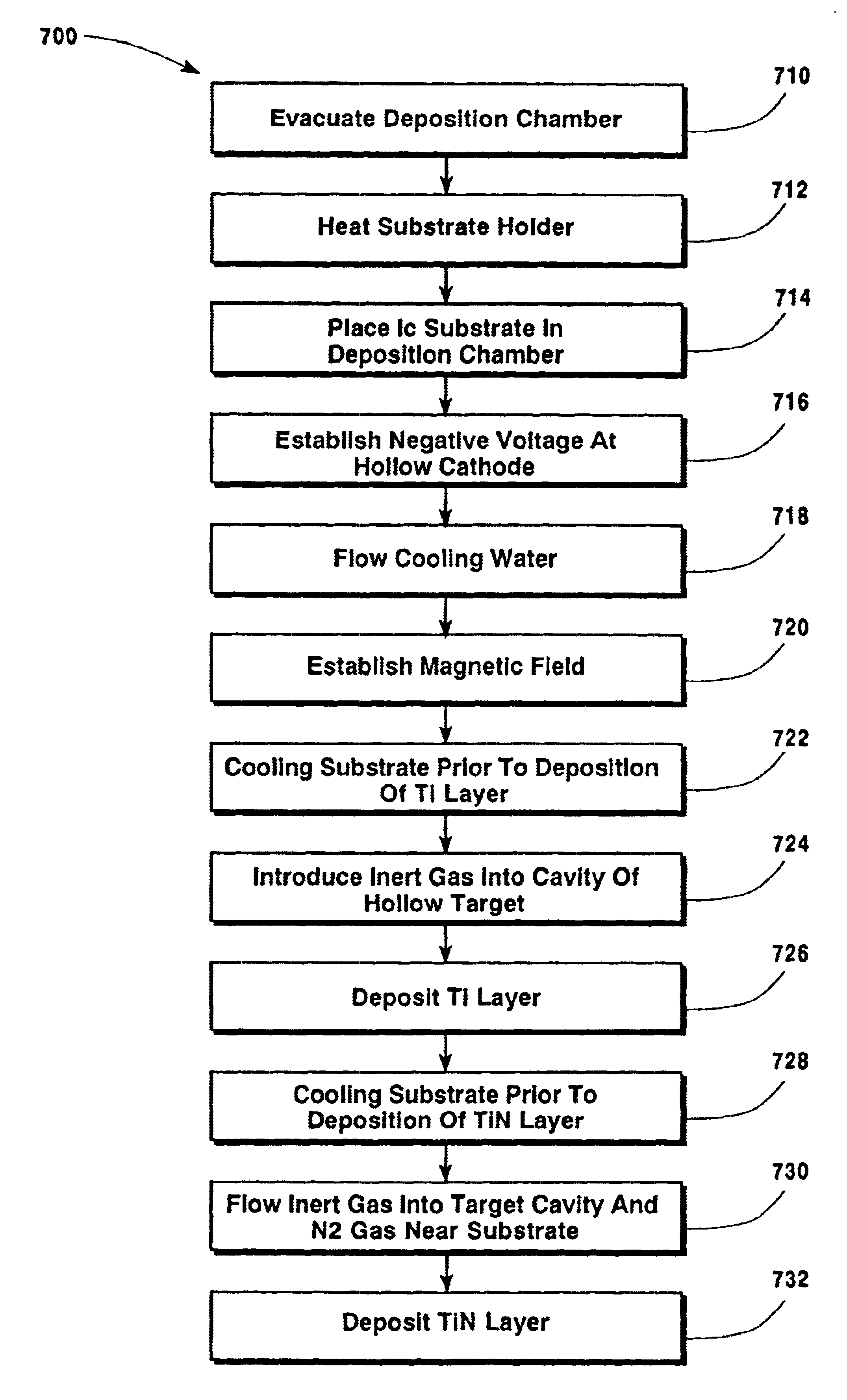
The present invention provides the use of incorporating a cooling step in the depositions processes of a titanium (Ti) liner film and a titanium nitride (TiN) barrier film in the same chamber to modulate and improve the via and contact resistance, without the use of a collimator or a shutter, using a hollow-cathode magnetron ("HCM"). In accordance with the invention, a temperature controlled ESC is integrated into a deposition process of Ti and TiN layers in a single chamber using an HCM, without the use of a collimator or a shutter, to modulate the temperature of the wafer for the process flow of such I-PVD Ti / TiN deposition in a cluster tool for semiconductor manufacturing applications.

In the preferred embodiment, the instant invention adds additional layers of functionality to the PVD deposition...


PUM

PropertyMeasurementUnit
Lengthaaaaaaaaaa
Lengthaaaaaaaaaa
Timeaaaaaaaaaa

Abstract

A method of depositing thin films comprising Ti and TiN within vias and trenches having high aspect ratio openings. The Ti and TiN layers are formed on an integrated circuit substrate using a Ti target in a non-nitrided mode in a hollow cathode magnetron apparatus in combination with controlling the deposition temperatures by integrating cooling steps into the Ti / TiN deposition processes to modulate the via and contact resistance. The Ti and TiN layers are deposited within a single deposition chamber, without the use of a collimator or a shutter.

Description

This application is related to U.S. patent application Ser. No. 10 / 060,724 (Attorney Docket No. NOVE100028000), filed the same day and assigned to the same assignee as the present application, the disclosure of which is incorporated herein by reference.1. Field of the InventionThe present invention relates to a method for depositing titanium (Ti) liner layers and titanium nitride (TiN) barrier layers for applications in semiconductor processing having improved via and contact resistance.2. Description of Related ArtIn the manufacture of semiconductor devices, metal conductive layers are patterned for the purpose of making interconnections between different points on the device. After formation of this patterned metal conductive layer an electrically insulative material is deposited over the metal conductive layer. Vias may then be etched in the insulative layer in positions where contacts are desired between conductive regions. A robust diffusion barrier, or liner, may then be depos...

Claims


Application Information

Patent Timeline
IPC IPC(8): C23C14/06C23C14/18H01L21/285H01L21/02H01L21/70H01L21/768
CPCC23C14/0641C23C14/185H01L21/28568H01L21/76843H01L21/2855
Inventor D'COUTO, GERARD C.TKACH, GEORGEWOITGE, MICHAELDANEK, MICHAL
Owner NOVELLUS SYSTEMS
Learn More