Method of manufacturing semiconductor having group II-group VI compounds doped with nitrogen

a technology of group ii-group vi and doped semiconductors, applied in the direction of basic electric elements, electrical equipment, semiconductor devices, etc., can solve the problems of high manufacturing cost, significant drawbacks, and limitations of copper us

Inactive Publication Date: 2005-02-08
UNIVERSITY OF TOLEDO
View PDF8 Cites 49 Cited by
  • Summary
  • Abstract
  • Description
  • Claims
  • Application Information

AI Technical Summary

Problems solved by technology

Single crystalline layers are often made with a molecular beam epitaxy (MBE) process (or other vapor deposition process), but the largest area of a substrate that can be practically covered using such processes is on the order of several square centimeters because it is limited by the size tri of single crystal substrates, which is an impractical size when considering the surface area required for economically practical solar cells.
Therefore, although single crystal photovoltaic materials can be used to generate conversion e...

Method used


Image

  • Method of manufacturing semiconductor having group II-group VI compounds doped with nitrogen
  • Method of manufacturing semiconductor having group II-group VI compounds doped with nitrogen
  • Method of manufacturing semiconductor having group II-group VI compounds doped with nitrogen

Examples


example i

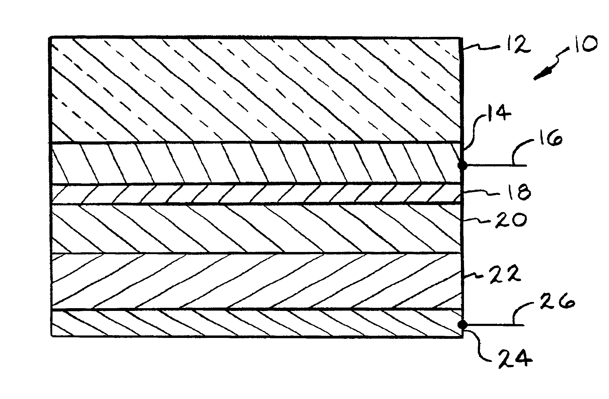
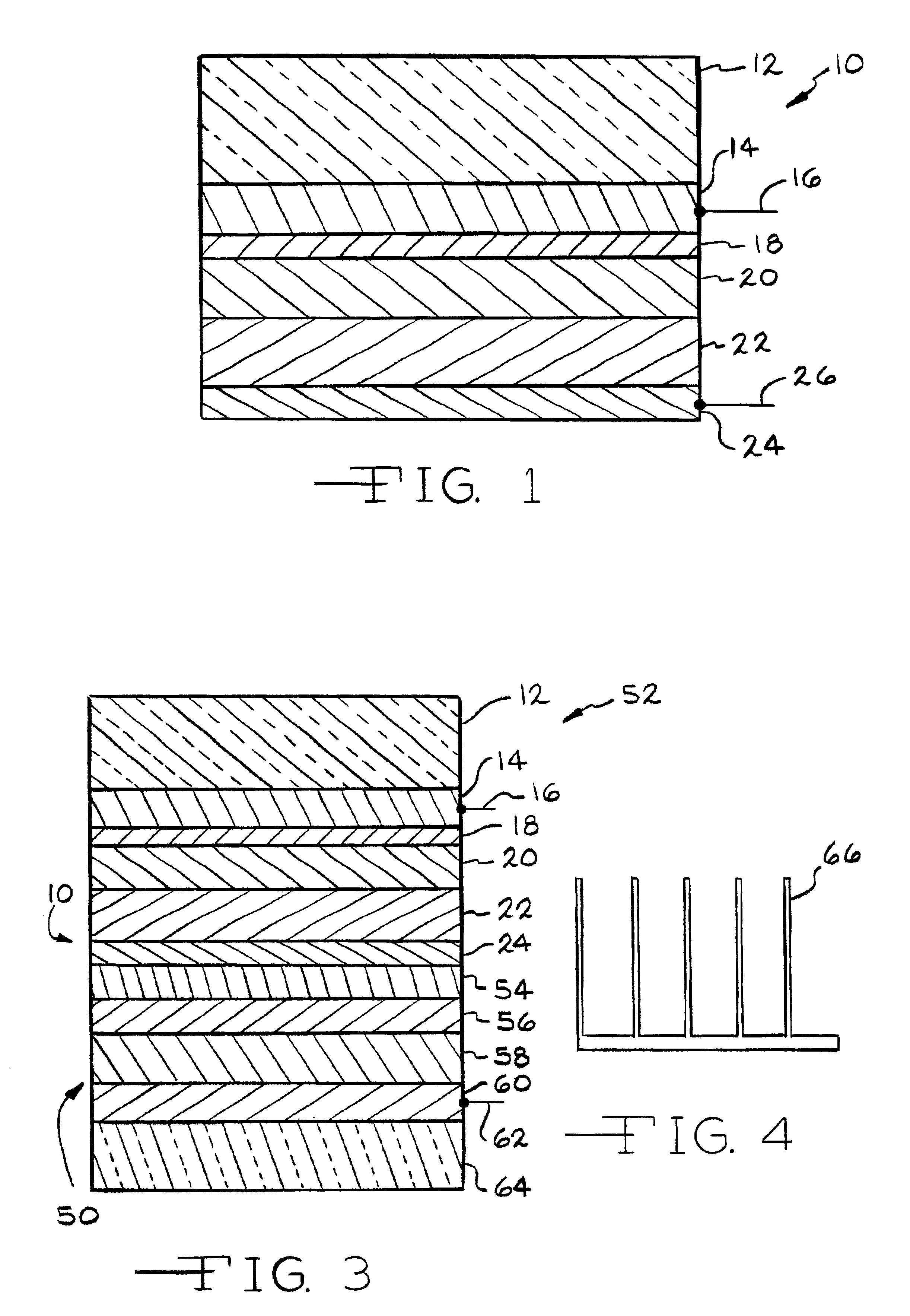
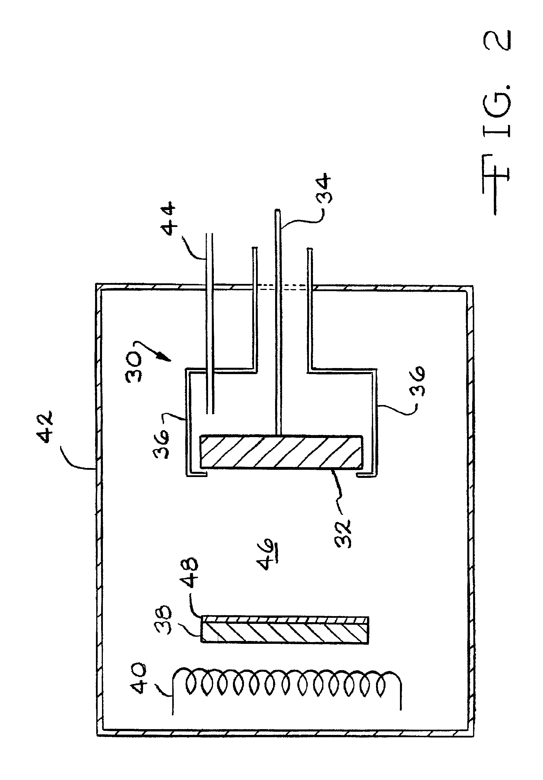
RF Sputtering was used to make a layer of nitrogen-doped zinc telluride in a solar cell. The reactive RF sputtering was carried out in a chamber assembled from a six-way stainless steel, copper gasketed cross with a two-inch planar magnetron mounted horizontally in one arm. The magnetron used an unbalanced magnetic field configuration. The substrate was suspended at the center of the cross about 2.5 inches from the sputter target in a heater assembly which provided radiant heating of the glass or tin dioxide (SnO2)-coated glass substrates. The preferred substrate temperature is within the range of from about 300 to about 400 degrees C. The gas flow, controlled by two parallel mass flow controllers, entered from another arm of the cross approximately in the plane of the substrate, although the gas injection can be made at the magnetron between the ground shroud (anode) and the target (cathode). In this example, the cadmium sulfide and cadmium telluride were previously deposited by a ...

example ii

The solar cell produced in Example I was tested for conversion efficiency, defined as the amount of electric energy produced as a percentage of the incident solar energy. When tested for conversion efficiency, the result was a conversion efficiency, of about 10 percent, when measured using an air mass 1.5 solar simulator.

example iii

The solar cell produced in Example I was tested for stability of the conversion efficiency. Two tests were conducted. For the first test, a set of solar cells was subjected to solar energy equivalent in intensity to the illumination provided by the sun, i.e., one-sun illumination, for a 24 hour per day, 125 day continuous exposure period, i.e., approximately 3,000 hours. The lamp used was a metal halide discharge lamp. The test was conducted under open circuit conditions at approximately 65 degrees C., with no current drawn from the cell. The test showed that the efficiency decreased about 15% over the first 1000 hours but then was stable. For the second test, a set of cells was subjected to heating at 100 degrees C. continuously in the dark for 3,000 hours. Again the efficiency dropped less than 15% during the first 1000 hours and then was stable. Similar cells with copper-based contacts lost half or more of their efficiency over this 3000 hour test. It can be seen that the efficie...


PUM


Abstract

A method of making a semiconductor comprises depositing a group II-group VI compound onto a substrate in the presence of nitrogen using sputtering to produce a nitrogen-doped semiconductor. This method can be used for making a photovoltaic cell using sputtering to apply a back contact layer of group II-group VI compound to a substrate in the presence of nitrogen, the back coating layer being doped with nitrogen. A semiconductor comprising a group II-group VI compound doped with nitrogen, and a photovoltaic cell comprising a substrate on which is deposited a layer of a group II-group VI compound doped with nitrogen, are also included.

Description

TECHNICAL FIELDThe present invention concerns semiconductor materials and methods of manufacturing semiconductor materials. More particularly, this invention relates to manufacturing semiconductor materials that are doped for improved formation of mobile charge carriers, particularly for such uses as in photovoltaic cells.BACKGROUND OF THE INVENTIONIt is well known that solar cells or photovoltaic cells can be used to convert solar energy into electric current. Typical photovoltaic cells include a substrate for mounting the cell and two ohmic contacts or conductors for passing current to an external electrical circuit. The cell also includes two or three semiconductor layers in series. The two layer type of semiconductor cell consists of an n-type layer and a p-type layer, and the three layer type includes an intrinsic (i-type) layer positioned between the n-type layer and the p-type layer for absorption of light radiation. The operate by having readily excitable electrons that can ...

Claims


Application Information

Patent Timeline
IPC IPC(8): H01L21/02H01L21/28H01L21/363H01L31/18
CPCH01L31/1828H01L21/02422H01L21/02474H01L21/02631H01L21/02502H01L21/02562H01L21/02579H01L21/02491Y02E10/543
Inventor COMPAAN, ALVIN D.PRICE, KENT J.MA, XIANDAMAKHRATCHEV, KONSTANTIN
Owner UNIVERSITY OF TOLEDO
Why Eureka
Try Eureka