
Method of fabricating nitride semiconductor device

Inactive Publication Date: 2005-03-15
PANASONIC CORP
View PDF24 Cites 17 Cited by
  • Summary
  • Abstract
  • Description
  • Claims
  • Application Information

AI Technical Summary

Benefits of technology

[0027]In consideration of the aforementioned conventional problems, an object of the invention is improving the crystal quality of a nitride semiconductor, particularly the crystal quality of an active region and its vicinity of a semiconductor light emitting device, so as to improve the operation characteristics such as luminous efficiency.

Problems solved by technology

As a result, there arises a problem that constituent elements are released (re-evaporated) from the crystal face.
This degradation results in lowering the luminous efficiency and degrading operation characteristics, for example, increasing a threshold current, of the resultant light emitting diode or semiconductor laser diode.
Accordingly, the material gases cannot be efficiently supplied onto the growth face of a crystal on the substrate, resulting in extremely lowering the growth rate or preventing magnesium (Mg), that is, the p-type dopant, from being introduced into the crystal.
Furthermore, when the flow rate of a carrier gas for carrying the material gases is increased for avoiding the production of the intermediate reaction product, the amount of gases flowing through a reaction tube is so large that vortexes and convections are caused in the air flow within the reaction tube.
As a result, the crystal cannot be grown under stable conditions.

Method used


Image

  • Method of fabricating nitride semiconductor device
  • Method of fabricating nitride semiconductor device
  • Method of fabricating nitride semiconductor device

Examples


embodiment 1

[0056

[0057]Embodiment 1 of the invention will now be described with reference to the accompanying drawings.

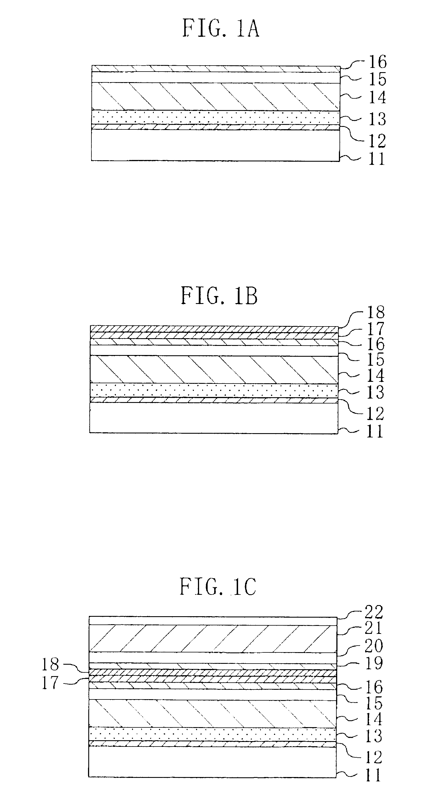
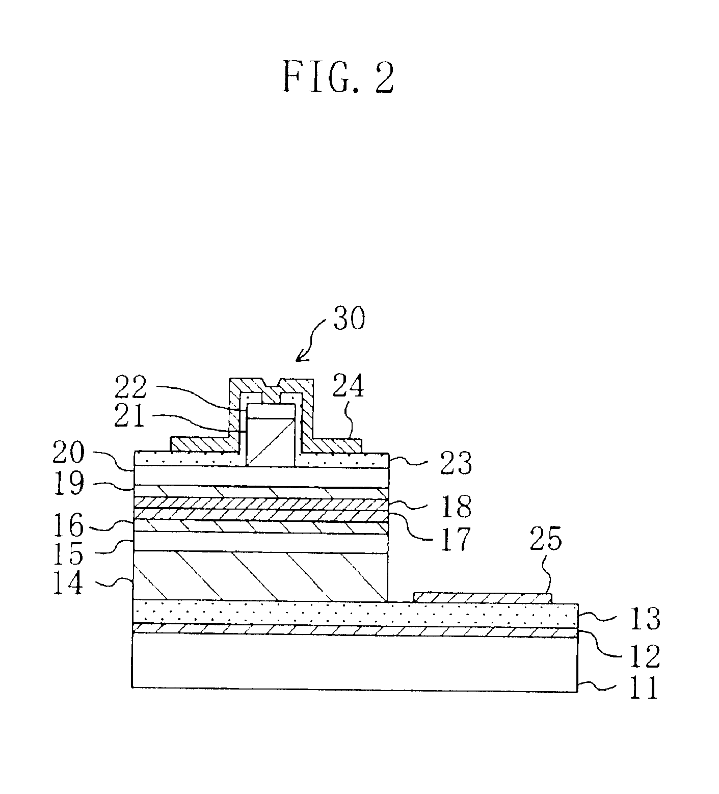
[0058]FIGS. 1(a) through 1(c) and 2 are sectional views for showing procedures in a method of fabricating a nitride semiconductor laser diode of Embodiment 1.

[0059]First, as is shown in FIG. 1(a), with a growth temperature set to approximately 500° C., trimethylgallium (TMG) serving as a gallium source and ammonia (NH3) serving as a nitrogen source are introduced onto a substrate 11 of sapphire by metal organic vapor phase epitaxial growth (MOVPE), so as to form a buffer layer 12 of GaN for relaxing lattice mismatch between sapphire and a gallium nitride-based semiconductor. Then, after the substrate temperature is increased to approximately 1020° C., TMG serving as a gallium source, trimethylaluminum (TMA) serving as an aluminum source, if necessary, NH3 serving as a nitrogen source and monosilane (SiH4) including silicon serving as an n-type dopant are introduced onto the sub...

embodiment 2

[0096

[0097]Embodiment 2 of the invention will now be described with reference to the accompanying drawings.

[0098]In Embodiment 1, in order to improve the crystal quality of an active layer and reduce products generated through the vapor phase intermediate reaction between material gases, the growth pressure is set to different values between the growth of the active layer and the growth of semiconductor layers sandwiching the active layer and having a smaller refractive index than the active layer. In Embodiment 2, another method for improving the quality of the active layer will be described.

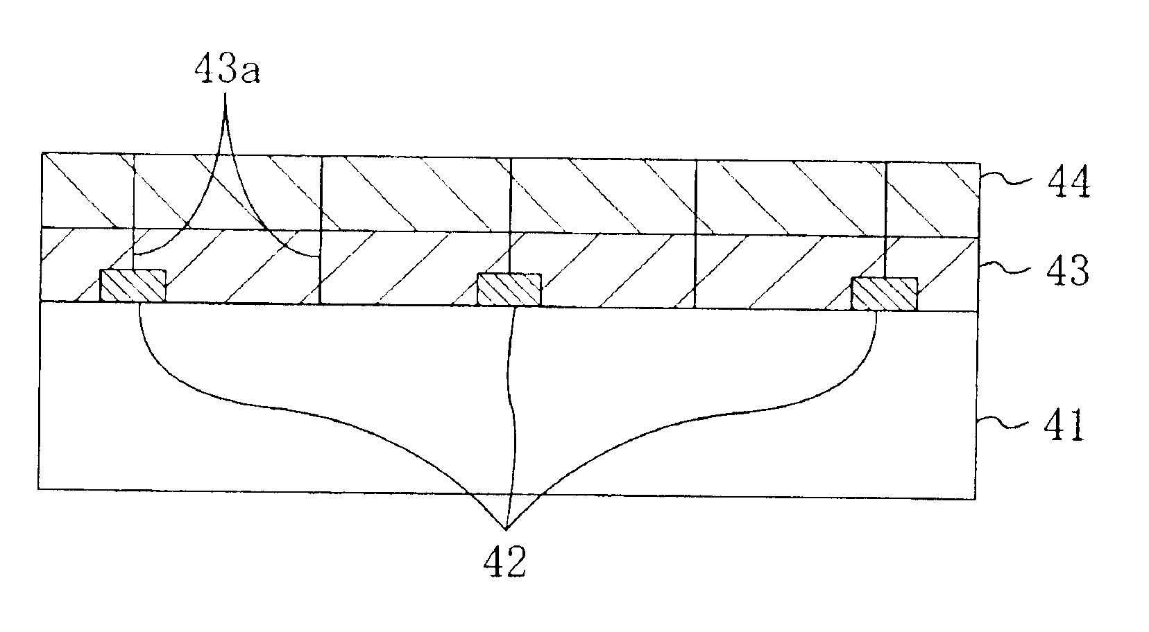
[0099]FIGS. 8 and 9 are sectional views for showing procedures in a method of fabricating a nitride semiconductor laser diode of Embodiment 2.

[0100]First, as is shown in FIG. 8, seed crystal layers 42 of GaN in the shape of plural ridge stripes extending at intervals are formed on a substrate of, for example, sapphire. The seed crystal layers 42 can be formed, for example, by growing a semicond...


PUM


Abstract

The method of fabricating a nitride semiconductor device of this invention includes plural steps of respectively growing plural nitride semiconductor layers on a substrate; and between a step of growing one nitride semiconductor layer and a step of growing another nitride semiconductor layer adjacent to the one nitride semiconductor layer among the plural steps, a step of changing a growth ambient pressure from a first growth ambient pressure to a second growth ambient pressure different from the first growth ambient pressure.

Description

BACKGROUND OF THE INVENTION[0002]The present invention relates to a method of fabricating a nitride semiconductor device such as a semiconductor laser diode expected to be applied to the fields of optical information processing and the like.[0003]Recently, a nitride semiconductor of a group III-V compound, that is, a compound including nitride (N) as a group V element, is regarded as a promising material for a short-wavelength light emitting device due to its large energy gap. In particular, a gallium nitride-based compound semiconductor (AlxGayInzN, wherein 0≦x, y, z≦1 and x+y+z=1) has been earnestly studied and developed, resulting in realizing a practical blue or green light emitting diode (LED) device. Furthermore, in accordance with capacity increase of an optical disk unit, a semiconductor laser diode lasing at a wavelength of approximately 400 nm is earnestly desired, and a semiconductor laser diode using a gallium nitride-based semiconductor is to be practically used.[0004]N...

Claims


Application Information

Patent Timeline
IPC IPC(8): H01L21/20H01L21/205H01L21/02H01S5/343H01S5/00H01L33/00H01S5/323
CPCH01S5/32341H01L21/02378H01L21/02381H01L21/02645H01L21/02458H01L21/0254H01L21/02576H01L21/0262H01L21/0242H01L33/007
Inventor ISHIBASHI, AKIHIKOKIDOGUCHI, ISAOHARAFUJI, KENJIBAN, YUZABURO
Owner PANASONIC CORP
Learn More