

Method of manufacturing a semiconductor device
- Summary
- Abstract
- Description
- Claims
- Application Information
AI Technical Summary
Benefits of technology
Problems solved by technology
Method used
Image

Examples
embodiment 1
[Embodiment 1]
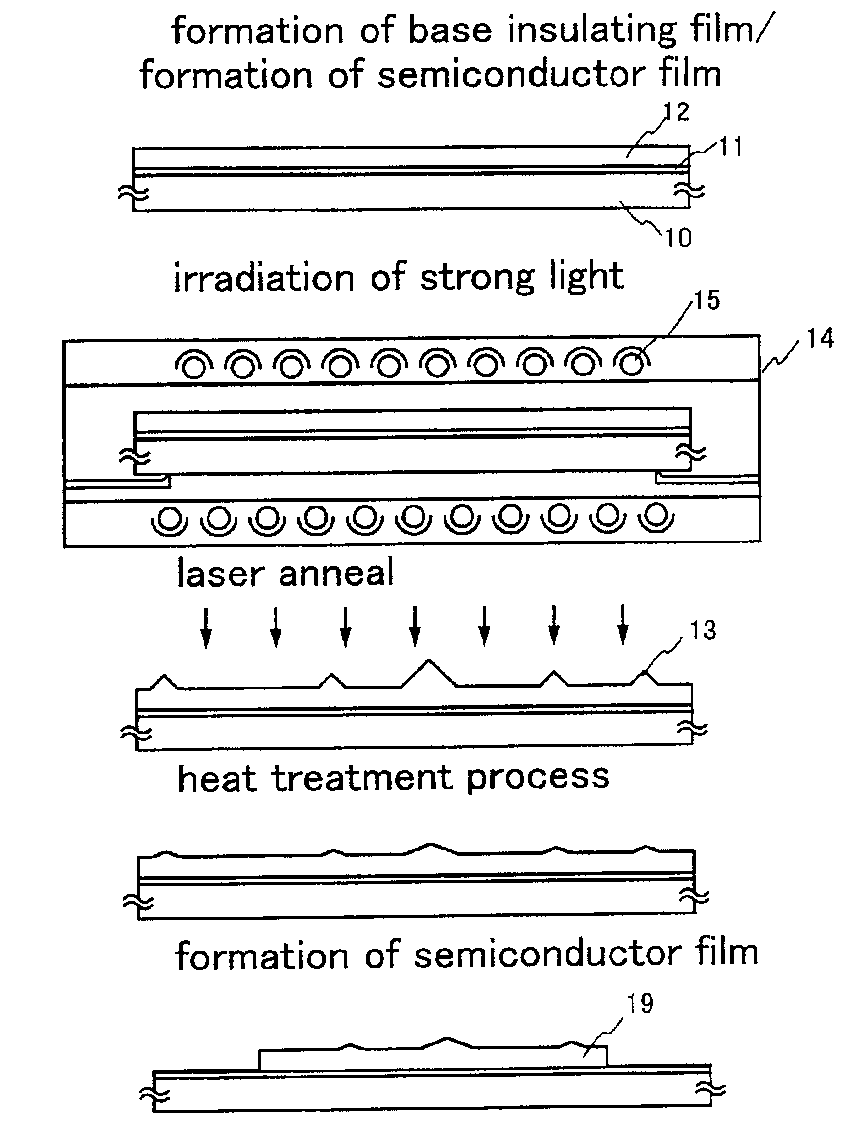
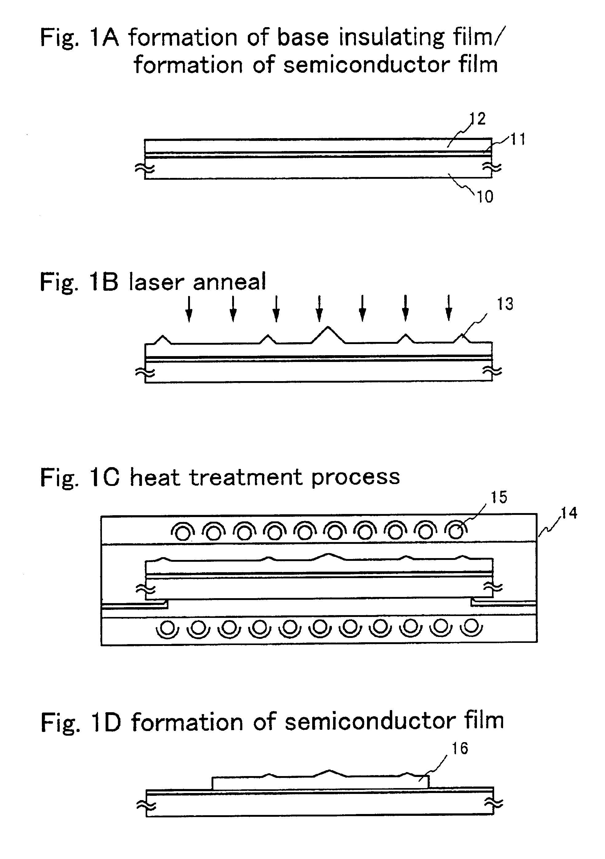
An embodiment of the present invention is explained using FIGS. 1A to 1D.
First, a base insulating film 11 is formed on a substrate 10. Substrates such as glass substrates and quartz substrates having light transmitting properties are used as the substrate 10. Further, an insulating film formed from a silicon oxide film, a silicon nitride film, a silicon oxynitride film, or the like is used as the base insulating film 11. An example is shown here of using a single layer structure as the base insulating film 11, but the insulating film may also have a structure in which two or more layers are laminated. Note that the base insulating film may not be formed. A glass substrate is used in this embodiment, and a silicon oxynitride film is formed to a film thickness of 150 nm on the glass substrate by using plasma CVD.
A semiconductor film 12 is formed next on the base insulating film 11. The semiconductor film 12 is formed using a known means (such as sputtering, LPCVD, or pla...
embodiment 2
[Embodiment 2]
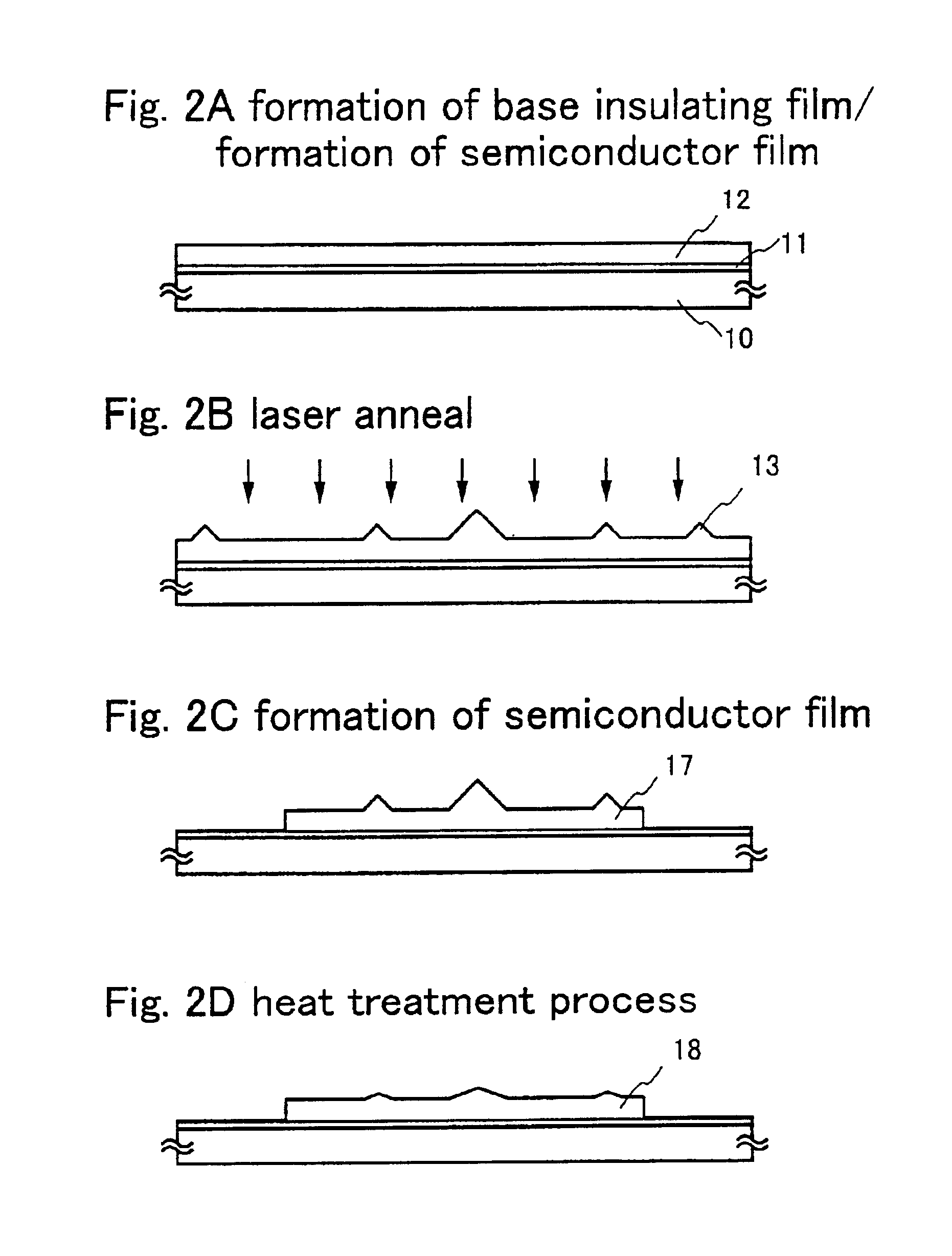
A method of reducing distortions of a semiconductor film that has undergone a manufacturing process differing from that of Embodiment 1 is explained in this embodiment using FIGS. 2A to 2D.
First, the state of FIG. 1A is manufactured in accordance with this Embodiment 1. Note that FIG. 1A and FIG. 2A show the same state, and that the same reference numerals are used in corresponding locations.
Laser crystallization is performed next to form a crystalline semiconductor film. Laser crystallization method may of course also be performed after using another known crystallization process (such as a thermal crystallization method). The second higher harmonic wave of a YAG laser is irradiated in this embodiment such that its light is formed into a linear shape on an irradiation surface by using an optical system. The crystallinity of the semiconductor film is thus increased, but the distortions 13 develop in the semiconductor film due to the laser light irradiation.
Patterning i...
embodiment 3
[Embodiment 3]
A method of reducing distortions of a semiconductor film that has undergone a manufacturing process differing from those of Embodiments 1 and 2 is explained in this embodiment using FIGS. 3A to 3E.
First, the state of FIG. 1A is manufactured in accordance with Embodiment 1. Note that FIG. 1A and FIG. 3A show the same state, and that the same reference numerals are used in corresponding locations.
A first heat treatment process is performed next, to crystallize the semiconductor film. RTA is used as the heat treatment process here. RTA may be performed, for example, by turning on the eleven halogen lamps (infrared light) 15 set below the substrate, and the ten halogen lamps 15 set above the substrate, between 1 and 10 times (preferably between 2 and 6 times) at a cycle length of 1 to 60 seconds (preferably between 30 and 60 seconds) in a nitrogen atmosphere. Heat supplied from the halogen lamps is between 700 and 1300° C. (measured by a thermocouple embedded in a silicon ...
PUM
| Property | Measurement | Unit |
|---|---|---|
| Temperature | aaaaa | aaaaa |
| Temperature | aaaaa | aaaaa |
| Temperature | aaaaa | aaaaa |
Abstract
Description
Claims
Application Information