Fabrication of semiconductor devices with transition metal boride films as diffusion barriers

a technology of transition metal boride and semiconductor devices, which is applied in the direction of crystal growth process, chemically reactive gas, chemistry apparatus and processes, etc., can solve the problems of device degradation and saturation current drop, and achieve the effect of improving the properties of the devi

Inactive Publication Date: 2005-03-29
MICRON TECH INC
View PDF38 Cites 45 Cited by
  • Summary
  • Abstract
  • Description
  • Claims
  • Application Information

AI Technical Summary

Benefits of technology

In general, techniques are disclosed for fabricating semiconductor devices and integrated circuits incorporating a transition metal boride layer. The transition metal boride layer can act as a diffusion barrier to improve the properties of the device.

Problems solved by technology

The additional oxide can cause device degradation, such as a shift in the threshold voltage and a decrease in the saturation current.

Method used


Image

  • Fabrication of semiconductor devices with transition metal boride films as diffusion barriers
  • Fabrication of semiconductor devices with transition metal boride films as diffusion barriers
  • Fabrication of semiconductor devices with transition metal boride films as diffusion barriers

Examples


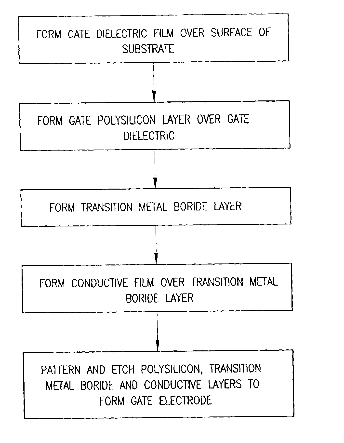
Embodiment Construction

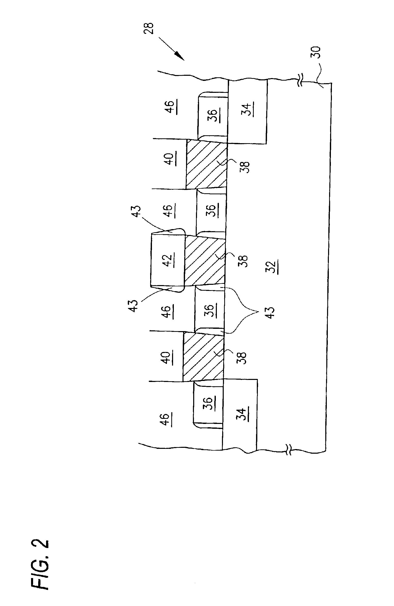
Referring to FIG. 2, an integrated circuit includes a DRAM cell 28. The DRAM 28 is formed on a silicon substrate 30 with an active region 32 and shallow trench isolation regions 34. Multiple word line or gate stacks 36 are formed over the active region 32 as well as over the isolation regions 34, and are separated by polysilicon plugs 38 and dielectric spacers 43. Capacitive cells 40 are provided above some of the polysilicon plugs 38, and a digit line stack 42 is formed over another one of the plugs. A passivation layer 46 comprising boro-phospho silicate glass (BPSG) can be provided over the surface of the device.

Referring to FIGS. 3 and 6, further details of the gate stacks 36 are described. A gate dielectric layer 54 is provided on the surface of the monocrystalline silicon substrate 30 which may include other previously-formed layers. In some implementations, the gate dielectric 54, which can comprise, for example, a deposited or thermally grown silicon oxide (SiO2) layer, has ...


PUM

PropertyMeasurementUnit
thicknessaaaaaaaaaa
thicknessaaaaaaaaaa
dielectric constantaaaaaaaaaa

Abstract

An integrated circuit has a multi-layer stack such as a gate stack or a digit line stack disposed on a layer comprising silicon. A conductive film is formed on the transition metal boride layer. A process for fabricating such devices can include forming the conductive film using a vapor deposition process with a reaction gas comprising fluorine. In the case of a gate stack, the transition metal boride layer can help reduce or eliminate the diffusion of fluorine atoms from the conductive film into a gate dielectric layer. Similarly, in the case of digit line stacks as well as gate stacks, the transition metal boride layer can reduce the diffusion of silicon from the polysilicon layer into the conductive film to help maintain a low resistance for the conductive film.

Description

BACKGROUNDThe present invention relates generally to semiconductor devices and, more particularly, to the use of transition metal boride films as diffusion barriers in devices such as gate stacks and digit line stacks.In some semiconductor memory circuits, word lines, which are formed from a uniformly-thick conductive layer, form both gate electrodes and gate interconnections. Whenever a word line passes over a field-oxide region, it functions as a gate electrode interconnection; whenever the word line passes over a gate dielectric layer overlaying an active region, it functions as a gate electrode.In early generations of integrated circuits, gate electrodes and electrode interconnections were often etched from a heavily-doped polycrystalline silicon (polysilicon) layer. To achieve increased operational speeds and lower stack heights-in subsequent generations of circuits, it was necessary to decrease the sheet resistance of the conductive layer from which the gates and gate intercon...

Claims


Application Information

Patent Timeline
Patent Type & Authority Patents(United States)
IPC IPC(8): H01L23/52H01L21/28H01L21/02H01L23/532H01L21/3215H01L29/40H01L29/49
CPCH01L21/28061H01L21/2807H01L21/28079H01L21/28088H01L21/28097H01L29/4975H01L21/3215H01L23/53266H01L29/4941H01L29/495H01L29/4966H01L21/28105H01L2924/0002H01L2924/00
Inventor DEBOER, SCOTT J.AL-SHAREEF, HUSAM N.
Owner MICRON TECH INC
Why Eureka
Try Eureka