Method of forming oxynitride film or the like and system for carrying out the same

a technology of oxynitride and film, which is applied in the field of forming oxynitride films or the like, can solve the problems of difficult to form an oxynitride film having a desired nitrogen content, the uniformity of intrasurface thickness is worse, and the nitrogen gas cannot be satisfactorily pyrolyzed, etc., to achieve the effect of high film forming rate and promotion of silane gas oxidation in the reaction chamber

Inactive Publication Date: 2005-04-26
TOKYO ELECTRON LTD
View PDF30 Cites 312 Cited by
  • Summary
  • Abstract
  • Description
  • Claims
  • Application Information

AI Technical Summary

Benefits of technology

[0058]According to another feature of the present invention, a silicon dioxide film forming system comprises: a reaction vessel defining a reaction chamber that can contain an object to be processed having a surface provided with at least a silicon layer; a reaction chamber heating unit that can heat the reaction chamber to a predetermined temperature; a reaction chamber pressure regulating unit that can regulate pressure in the reaction chamber to a predetermined pressure; a first gas supplying unit that supplies a silane gas into the reaction chamber; a second gas supplying unit that supplies dinitrogen oxide gas into the reaction chamber; a gas heating unit, provided at the s

Problems solved by technology

However, if the process temperature is lowered, for example, from 900° C. to 800° C. or 750° C., nitrogen gas cannot satisfactorily be pyrolyzed and, consequently, it is difficult to form an oxynitride film having a desired nitrogen content.
Since a diameter of the wafer is increasing progressively, thickness uniformity of a film formed on the surface of the wafer, i.e., intrasurface thickness uniformity becomes worse when the process temperature is reduced.
In addition, thickness difference between films formed on the surfaces of the wafers, i.e., interwafer thickness uniformity also becomes worse.
The gas around an upper part of the wafer boat is not heated sufficiently.
Thus, it is inferred that the uniformity of the thickness of the films formed on the wafers held in the upper part of the wafer boat is considerably bad, and the difference between the thickness of the films formed on the wafers held in the upper part of the w

Method used


Image

  • Method of forming oxynitride film or the like and system for carrying out the same
  • Method of forming oxynitride film or the like and system for carrying out the same
  • Method of forming oxynitride film or the like and system for carrying out the same

Examples


experiment 1

(Experiment 1)

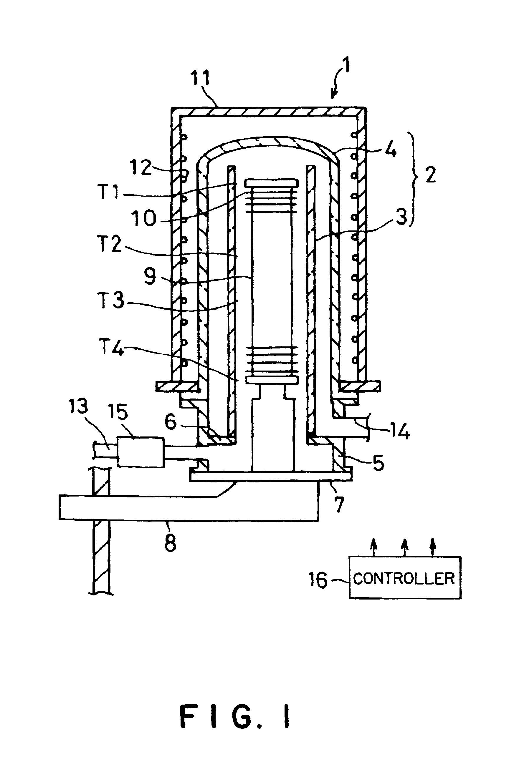
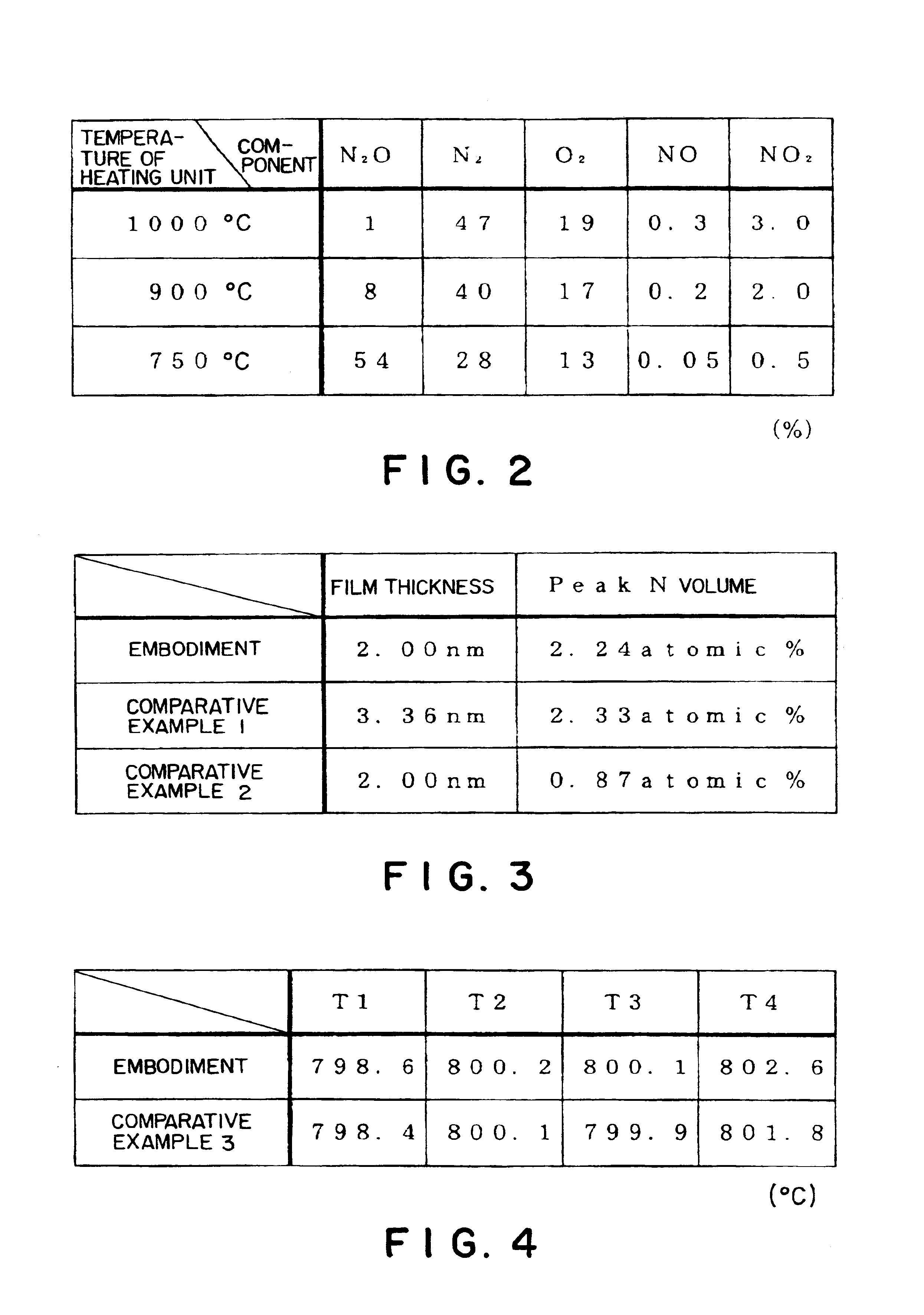
[0133]Silicon dioxide films were formed on the surfaces of 20 cm diameter wafers under the following process conditions, respectively.

[0134]Temperature in reaction tube: 800° C.

[0135]Flow rate of gases: O2 / HCl=10 / 0.5 slm

[0136]Processing time: 90 min

[0137]Temperature of heating unit: 1000° C.

[0138]Number of wafers on wafer boat: 100

[0139]Pressure in reaction tube: −49 Pa (−5 mmH2O)

[0140]The thickness of silicon oxide films formed on the wafers in upper, middle and lower parts, respectively, of the wafer boat was measured to examine the intrasurface thickness uniformity of the silicon dioxide films. In addition, silicon dioxide films were formed on the surfaces of wafers under process conditions similar to the foregoing process conditions, except that the heating element of the heating unit was not energized. FIG. 9 shows the measured results. Intrasurface thickness uniformity is represented by a value calculated by using:

[{(Maximum thickness)−(Minimum thickness)} / 2×(Mea...

experiment 2

(Experiment 2)

[0142]Silicon dioxide films were formed on the surfaces of 20 cm diameter wafers under the following process conditions, respectively.

[0143]Temperature in reaction tube: 800° C.

[0144]Flow rate of gases: O2 / HCl=10 / 0.3 slm

[0145]Temperature of heating unit: 1000° C.

[0146]Number of wafers on wafer boat: 100

[0147]Pressure in reaction tube: −49 Pa (−5 mmH2O)

[0148]Processing time: 2, 15, 30, and 60 min

[0149]Intrasurface thickness uniformity of the wafers held in a middle part of the wafer boat was examined. Interwafer thickness uniformity was also examined. FIG. 10 shows the results of examinations. Interwafer thickness uniformity is represented by a value calculated by using:

(A / 2×B)×100 (%)

where A is the difference between the maximum and the minimum among the respective mean thicknesses of the silicon dioxide films formed on the wafers held on the wafer boat (practically, a predetermined number of monitor wafers held on the wafer boat) and B is the mean of the respective m...

experiment 3

(Experiment 3)

[0151]An empty wafer boat was loaded into the reaction tube, the interior of the reaction tube was heated to 800° C., and oxygen gas and hydrogen chloride gas were supplied at 10 slm and 1 slm, respectively. The hydrogen concentration of the gas discharged through the exhaust pipe was measured while the system was operating in an operating mode with the heating element energized to heat the process gas at 1000° C. and in an operating mode with the heating element not energized.

[0152]FIG. 11 shows the measured results, in which preparatory time signifies a length of time for which the gas was supplied before starting analysis. It is known from FIG. 11 that the hydrogen concentration of the discharged gas is small when the process gas is heated by the heating unit. It is inferred that the reaction: H2+½O2 →H2O is promoted when the process gas is heated.

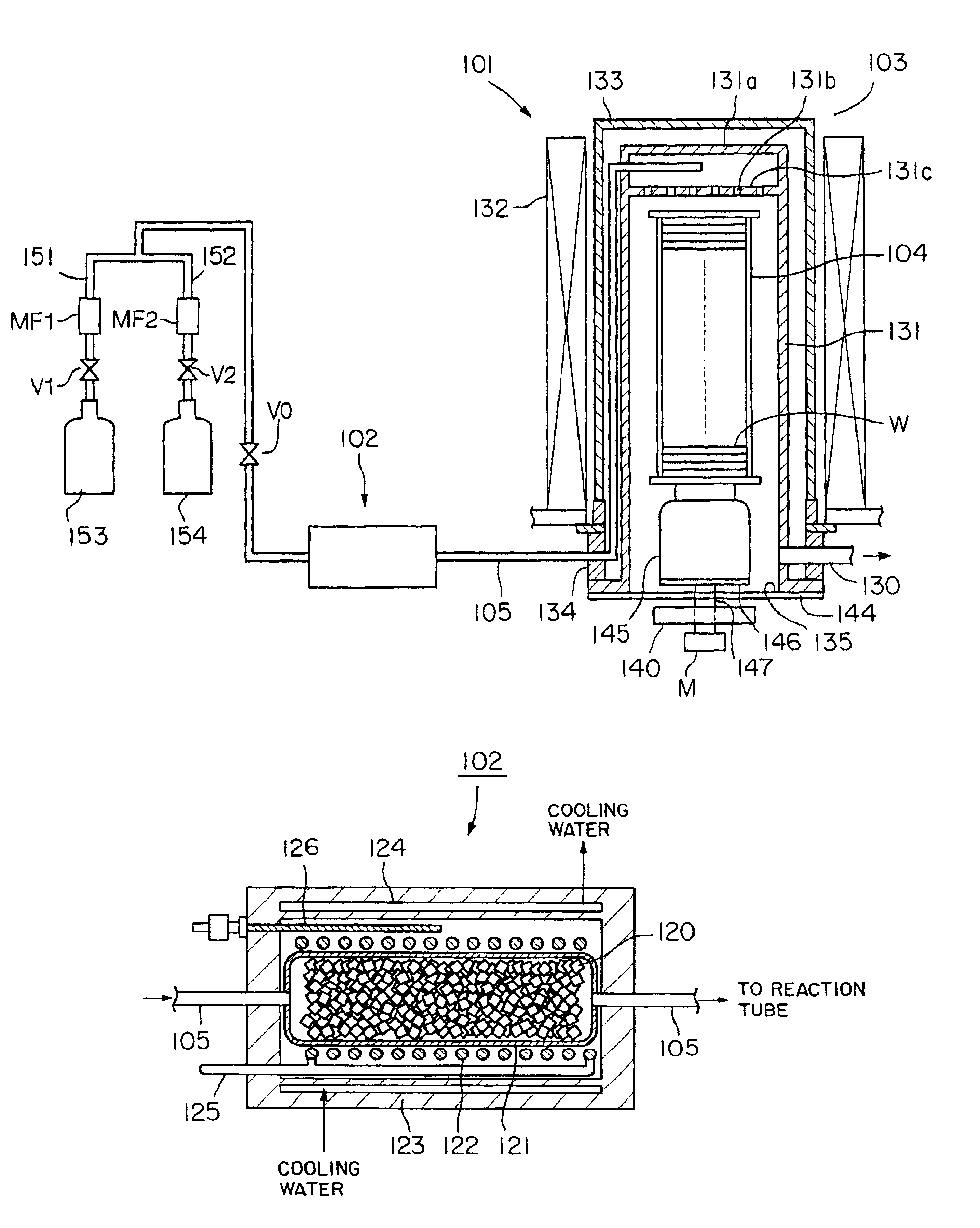
[0153]A system for forming a silicon nitride film and a method of forming a silicon nitride film in a third embodiment a...


PUM

PropertyMeasurementUnit
Temperatureaaaaaaaaaa

Abstract

This invention is an oxynitride film forming method including: a reaction chamber heating step of heating a reaction chamber to a predetermined temperature, the reaction chamber containing an object to be processed; a gas heating step of heating a process gas to a temperature not lower than a reaction temperature at which an oxynitride film can be formed, the process gas consisting of dinitrogen oxide gas; and a film forming step of forming an oxynitride film on the object to be processed by supplying the heated process gas into the heated processing chamber. The temperature to which the reaction chamber is heated in the reaction chamber heating step is set at a temperature below a temperature at which the process gas undergoes a reaction.

Description

BACKGROUND OF THE INVENTION[0001]1. Field of the Invention[0002]The present invention relates to a method of forming an oxynitride film or the like and a system for carrying out the same. More specifically, the present invention relates to a method of forming an oxynitride film or the like on an object to be processed, such as a semiconductor wafer, and a system for carrying out the same.[0003]2. Description of the Related Art[0004]A semiconductor device fabricating process forms an insulating film on an object to be processed, such as a semiconductor wafer. This insulating film is used, for example, as a mask for impurity diffusion or ion implantation or as a source of an impurity. A silicon oxynitride film is used occasionally as such an insulating film. Silicon oxynitride films, as compared with prevalently used silicon oxide films, have a high dielectric constant and have a high capability of preventing penetration by an impurity, such as boron.[0005]A silicon oxynitride film is...

Claims


Application Information

Patent Timeline
IPC IPC(8): H01L21/318H01L21/02H01L21/314H01L21/316
CPCH01L21/0214H01L21/02164H01L21/0217H01L21/02211H01L21/02238H01L21/3185H01L21/02255H01L21/02271H01L21/3144H01L21/31662H01L21/02249H01L21/67017H01L21/67103
Inventor ISHII, KATSUTOSHIMIURA, KAZUTOSHI
Owner TOKYO ELECTRON LTD
Why Eureka
Try Eureka