
Barrier structures for integration of high K oxides with Cu and Al electrodes

a barrier structure and high k oxide technology, applied in the field of new materials, can solve the problems of limited availability for use in semiconductor production environments, difficult etching or polishing of materials, and high cost of noble metal alloys and oxides, and achieve excellent conductivity and high melting point

Inactive Publication Date: 2005-05-31
ENTEGRIS INC
View PDF28 Cites 36 Cited by
  • Summary
  • Abstract
  • Description
  • Claims
  • Application Information

AI Technical Summary

Benefits of technology

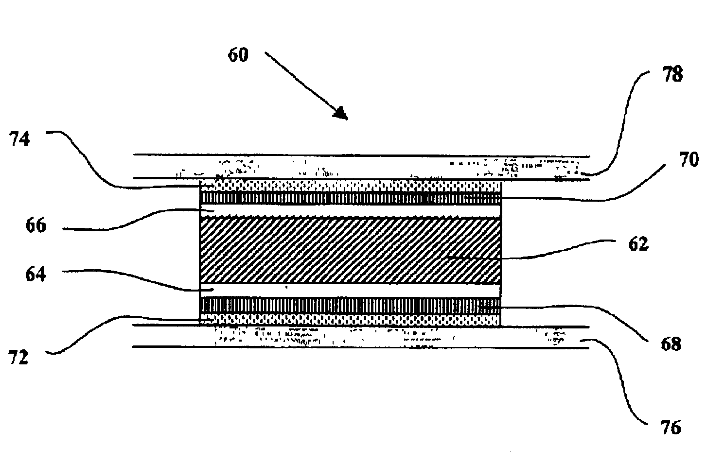
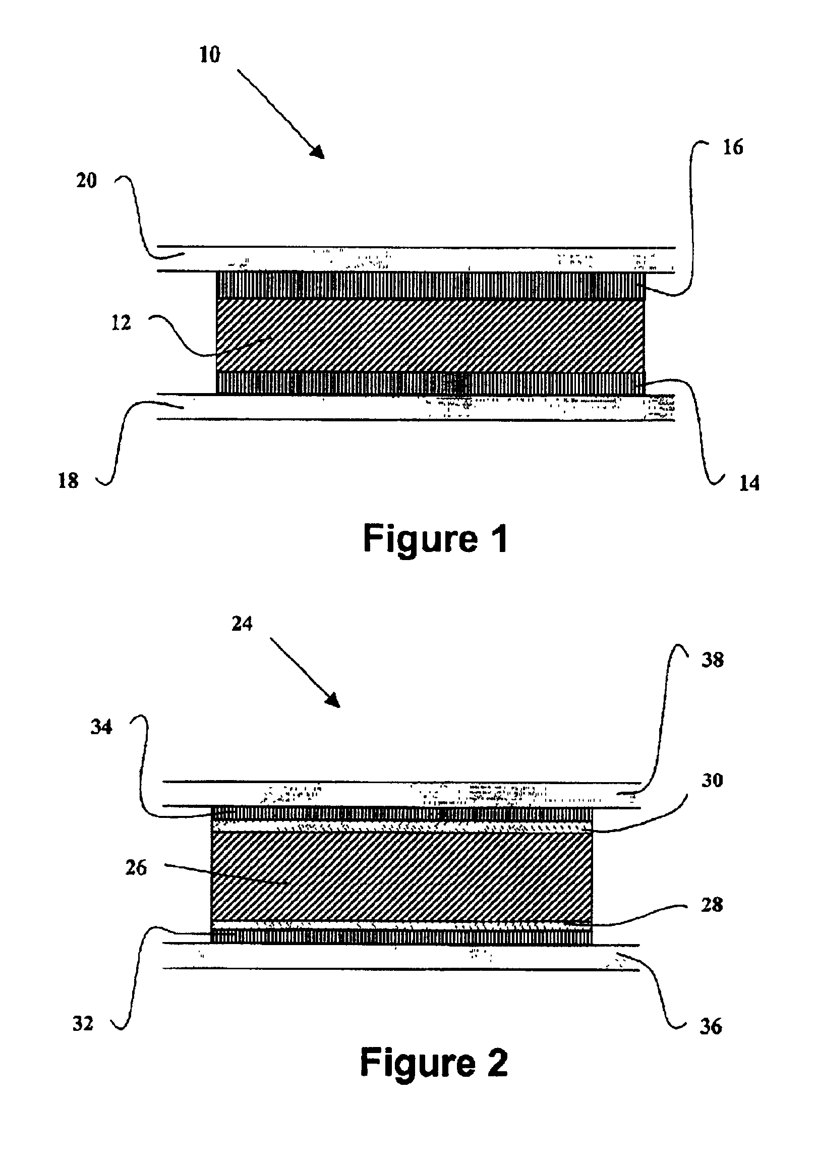
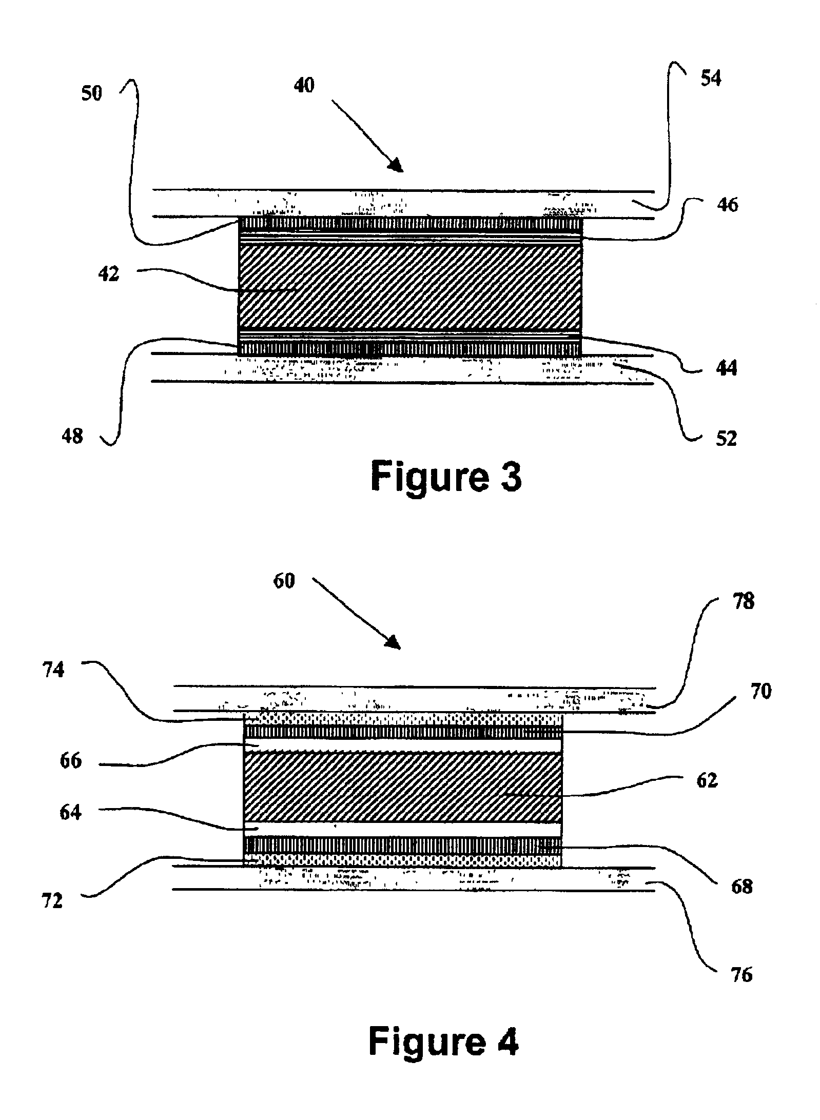
[0029]The conductive barrier layer may comprise a single layer of barrier materials. Double-layer and triple-layer structures can also be formed for enhanced diffusion resistance and better adhesion with the high dielectric constant material layer as well as with the metal electrode layer.

Problems solved by technology

Unfortunately, such noble metals, noble metal alloys and oxides are very expensive and of limited availability for use in semiconductor production environments.
Moreover, such materials are very difficult to etch or to polish, and they require etching or polishing compositions of very strong acidity or corrositivity.
Handling compositions of such strong acidity or corrositivity in turn increases the operating costs of the semiconductor manufacturing facility.
Discharge of such etching or polishing compositions after the semiconductor manufacturing process also leads to significant environmental problems and / or treatment costs.
Further, such noble metals, alloys, and oxides, especially Pt and Pt alloys, have relatively low conductivity.
However, both aluminum and copper have relatively high oxidization potentials and low oxidization resistances.
They also are subject to rapid oxidization in a high-temperature, oxidizing environment.
This in turn has adverse implications for the conventional method of forming the high dielectric constant oxide material, chemical vapor deposition (CVD).
Electrodes comprising aluminum or copper cannot maintain their integrity under such chemical vapor deposition processes.
This circumstance renders it difficult to use aluminum or copper electrodes in combination with high k metal oxide thin films.
Further, even without exposure to the chemical vapor deposition process, aluminum or copper is still susceptible to being oxidized at the Cu,Al / high k metal oxide interface, by oxygen diffusion through such interface.
Typical electrical property changes include, but are not limited to, increased leakage and energy loss.
Severe leakage and energy loss will in turn cause catastrophic breakdown (i.e., a short-circuit) between the electrodes and render the capacitor useless.

Method used


Image

  • Barrier structures for integration of high K oxides with Cu and Al electrodes
  • Barrier structures for integration of high K oxides with Cu and Al electrodes
  • Barrier structures for integration of high K oxides with Cu and Al electrodes

Examples


example 1

[0081]Amorphous BiTaO4 films are deposited onto two types of substrates: 100 nm Ir on 500 SiO2 on (100) Si and 10 nm TiAlN on 100 nm Ir on 500 nm SiO2 on (100) Si. In both cases the film thickness was determined by calibrated X-ray Fluorescence (XRF) using a mixture of the ideal densities for Bi2O3 and Ta2O5 to calculate thickness. Top electrodes of 100 nm Pt were deposited by electron beam evaporation through a shadow mask to define pads between 10−4 to 10−3 cm2 in area. The capacitance was measured using a HP4192A meter. The capacitance per unit area is shown in FIG. 5 as a function of dielectric film thickness for both electrode structures. Surprisingly, equivalent capacitance values for the same thickness of dielectric film were observed, indicating that there are no capacitive interlayers formed between the dielectric and the TiAlN interlayer.


PUM

PropertyMeasurementUnit
thicknessaaaaaaaaaa
thicknessaaaaaaaaaa
dielectric constantaaaaaaaaaa

Abstract

An integrated circuit barrier structure disposed between high dielectric constant metal oxide and Cu or Al electrodes, for preventing diffusion of species such as oxygen, bismuth, or lead from the high dielectric constant metal oxide into the Cu or Al electrodes. Such barrier structure also protects the Cu or Al electrodes against oxidization during deposition of the high dielectric constant metal oxide. The barrier structure can be formed as (1) a single layer of Pt, Ir, IrO2, Ir2O3, Ru, RuO2, CuO, Cu2O, Al2O3, or a binary or ternary metal nitride, e.g., TaN, NbN, HfN, ZrN, WN, W2N, TiN, TiSiN, TiAlN, TaSiN, or NbAlN, or (2) double or triple layers of such materials, e.g., Pt / TiAlN, Pt / IrO2, Pt / Ir, Ir / TiAlN, Ir / IrO2, IrO2 / TiAlN, IrO2 / Ir, or IrO2 / Ir2O3 / Ir. Such barrier structures enable Cu or Al electrodes to be used in combination with high dielectric constant metal oxides in microelectronic structures such as ferroelectric stack and trench capacitors, non-volatile ferroelectric memory cells, and dynamic random access memory (DRAM) cells.

Description

BACKGROUND OF INVENTION[0001]1. Field of the Invention[0002]The present invention relates to novel conductive barrier structures useful in integrated circuit memory cells, integrated capacitors for decoupling, integrated RC-matching networks or other electronic devices requiring high specific capacitance. In specific aspects, the present invention relates to microelectronic structures, e.g. including such conductive barrier layers between complex metal oxides of high dielectric constant and respective Cu or Al electrodes.[0003]2. Description of the Related Art[0004]Barrier layers are crucial components in many integrated circuits. Barrier layers are typically used to prevent interfacial diffusion of oxidizing species, silicon, metals, hydrogen, etc., while concurrently maintaining desired conductance / resistance characteristics in the integrated circuit structure.[0005]Integrated circuit memory devices, such as dynamic random access memories (DRAMs), include storage cells comprising ...

Claims


Application Information

Patent Timeline
Patent Type & Authority Patents(United States)
IPC IPC(8): H01L21/02H01L21/28
CPCH01L21/28291H01L28/75H01L28/55H01L29/40111
Inventor STAUF, GREGORY T.HENDRIX, BRYAN C.ROEDER, JEFFREY F.CHEN, ING-SHIN
Owner ENTEGRIS INC
Learn More