

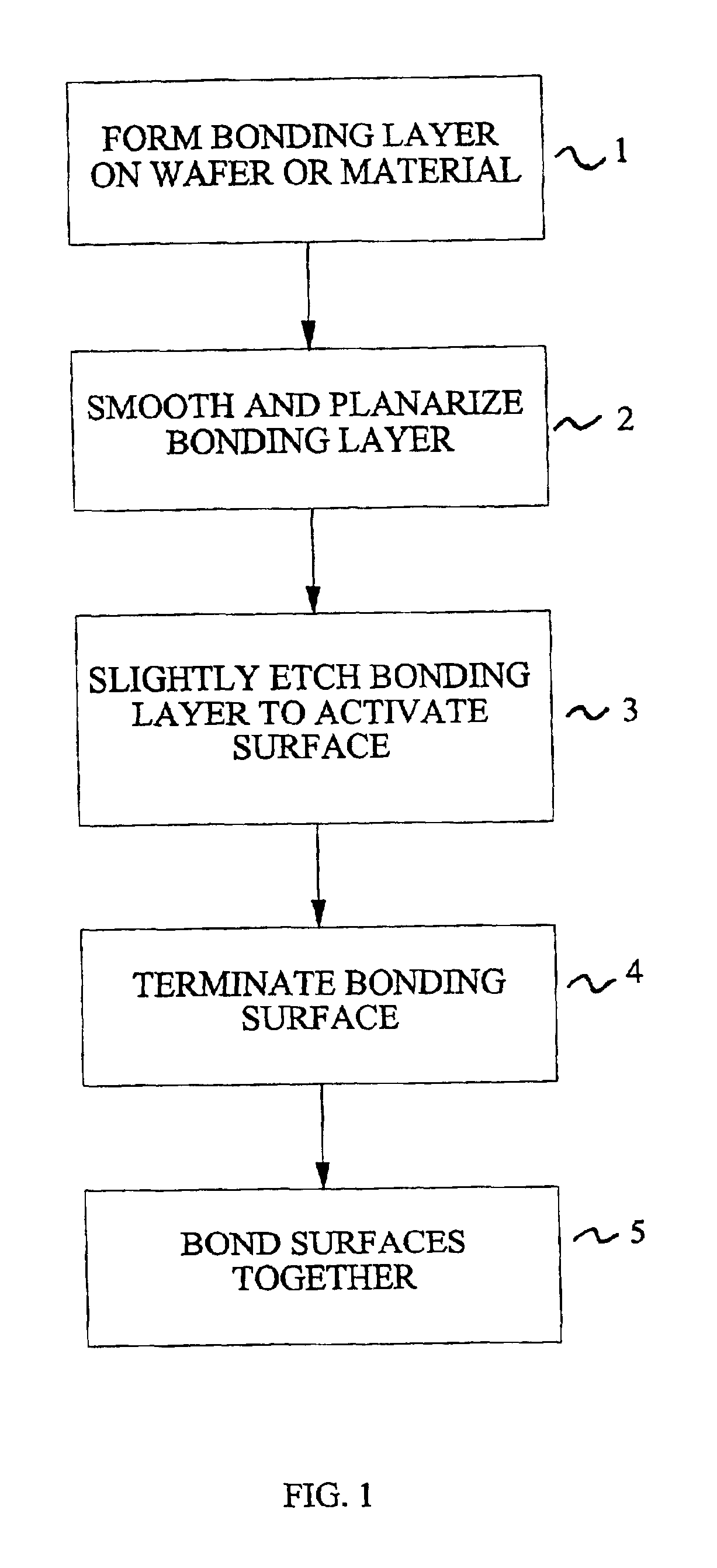
Method for low temperature bonding and bonded structure
a bonding and low temperature technology, applied in the direction of adhesives, semiconductor devices, electrical equipment, etc., can solve the problems of significantly limited wafer bonding applications, undesirable changes in the device or material being bonded, and the general failure of the uhv approach to work on commonly used materials, etc., to achieve the effect of increasing the bonding strength
- Summary
- Abstract
- Description
- Claims
- Application Information
AI Technical Summary
Benefits of technology
Problems solved by technology
Method used
Image

Examples
example 1
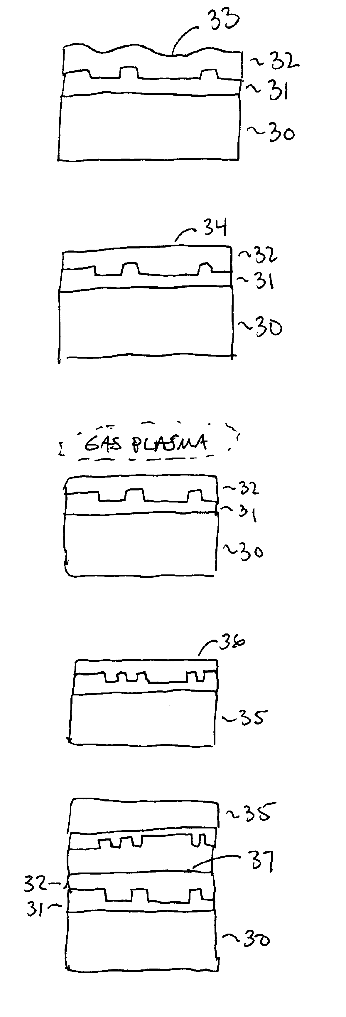
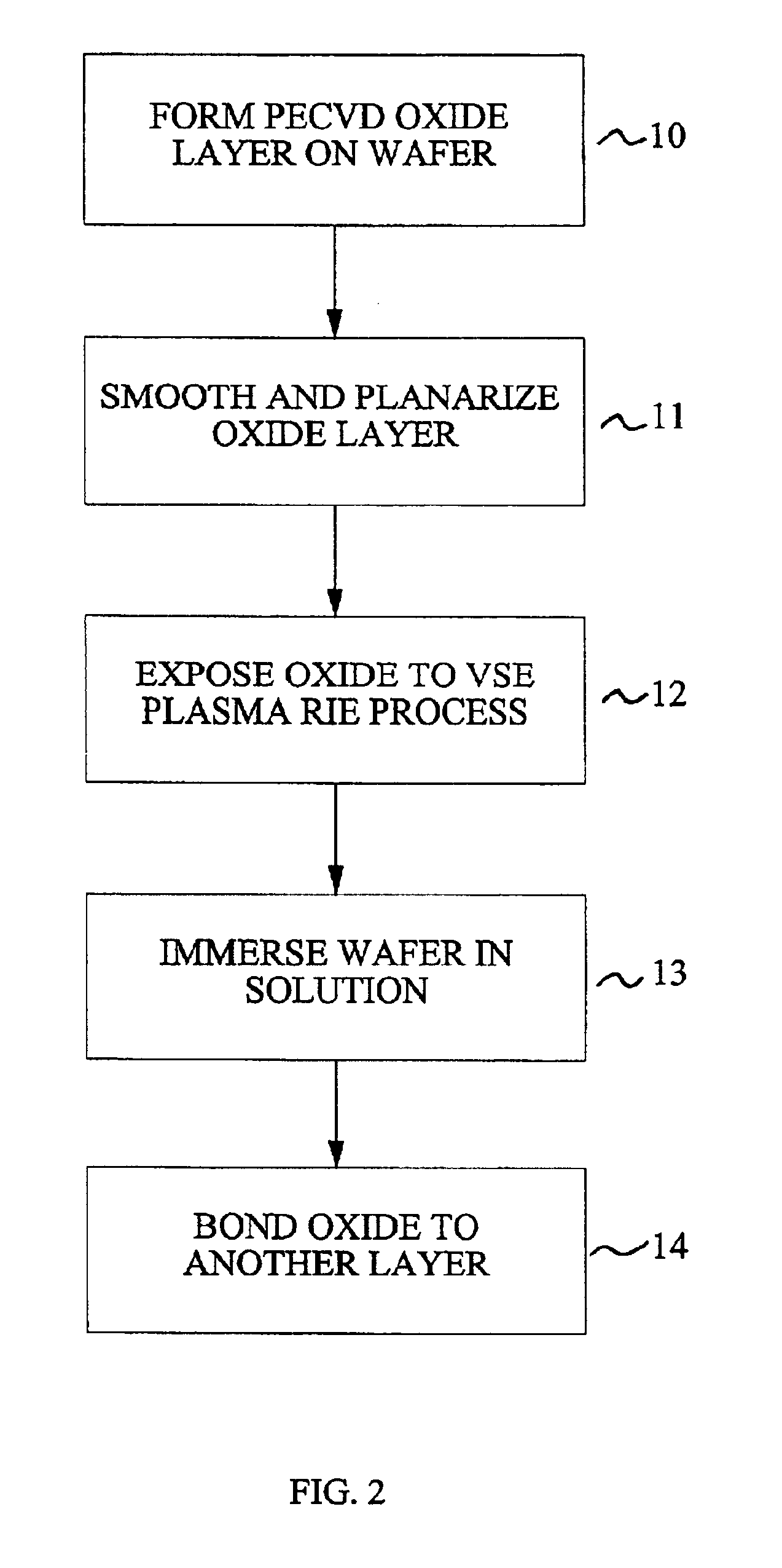
[0088]In a first example, three inch , 1-10 ohm-cm, boron doped silicon wafers were used. PECVD oxide was deposited on some of the silicon wafers. For comparison, thermal oxidized silicon wafers were also studied. The PECVD oxide thickness was 0.5 μm and 0.3 μm on the front side and the back side of the wafers, respectively. Oxide is deposited on both sides of the wafer to minimize wafer bow during polishing and improve planarization. A soft polish was performed to remove about 30 nm of the oxide and to smooth the front oxide surface originally having a root mean square of the micro-roughness (RMS) of ˜0.56 nm to a final ˜0.18 nm. A modified RCA1 solution was used to clean the wafer surfaces followed by spin-drying.
[0089]Two wafers were loaded into the plasma system, both wafers are placed on the RF electrode and treated in plasma in RIE mode. For comparison, some wafers were treated in plasma mode in which the wafers were put on the grounded electrode. An oxygen plasma was used wit...
examples 2-3
[0096]The above process was applied to bond processed InP wafers (600 μm thick) to AlN wafers (380 μm thick), or to bond processed Si (380 μm thick) and InP (600 μm thick) wafers, as second and third examples. The processed InP device wafers are covered with PECVD oxide and planarized and smoothed by chemical-mechanical polishing CMP. A PECVD oxide layer is also deposited on the AlN wafers and is planarized and smoothed to improve the RMS surface roughness. The processed Si and processed InP wafers are deposited with PECVD oxide and planarized and smoothed using CMP. After VSE similar to the example 1 bonding at room temperature, the bonded wafers are left in ambient air at room temperature.
[0097]After 24 hours storage at room temperature, bonding energy of 1000 mJ / m2 and 1100 mJ / m2 were achieved for the InP / Si and InP / AlN bonded pairs, respectively. For processed Si (380 μm thick) / oxide covered AlN (280 μm thick) wafer pairs, the bonding energy at room temperature as high as 2500 m...
PUM
| Property | Measurement | Unit |
|---|---|---|
| surface roughness | aaaaa | aaaaa |
| surface roughness | aaaaa | aaaaa |
| roughness | aaaaa | aaaaa |
Abstract
Description
Claims
Application Information