Bonded wafer with metal silicidation

a metal silicidation and bonding technology, applied in the direction of basic electric elements, electrical equipment, semiconductor devices, etc., can solve the problems of low quality of oxide, and general inferior quality of bulk silicon layer, so as to improve stress compensation, reduce warpage, and bond low temperature

Inactive Publication Date: 2005-06-21
INTERSIL CORP +1
View PDF32 Cites 25 Cited by
  • Summary
  • Abstract
  • Description
  • Claims
  • Application Information

AI Technical Summary

Benefits of technology

[0014]The present invention provides silicon-on-insulator bonded wafer processing with the features of (1) relatively low temperature bonding by the use of low temperature, about 500-800° C. metal silicidation reactions for bonding; (2) better stress compensation by providing materials in the bonding zone that will produce silicides with coefficients of thermal expansion closely matched to those of the substrate wafers and buried dielectric layers, thereby reducing warpage; (3) limiting contaminant migration by means of a bonding zone that provides a barrier to diffusion of mobile contaminants; (4) simultaneously producing a buried doped layer in the silicon during the bonding process; (5) a conductive, dielectrically-isolated layer at the bonding zone; and (6) a thermally conductive layer at the bonding zone.

Problems solved by technology

Scaling bulk devices tends to degrade their characteristics because of small-geometry effects such as punch-through, threshold voltage shift, and subthreshold-slope degradation.
However, the quality of such a silicon layer is generally inferior to that normally associated with bulk silicon.
Other approaches entail forming an oxide layer beneath an existing high quality silicon layer, either by oxidizing a buried porous silicon layer or by oxygen ion implantation; however, such oxide is low quality, and the silicon top layer may be damaged during the oxide layer formation.
Bonded wafers, however, have problems of high temperature bonding that lead to film stress and delamination.
Also, because oxides are poor diffusion barriers to mobile ions such as sodium, bonded wafers with silicon dioxide buried layers are susceptible to contaminant diffusion.
Contaminants introduced during the bonding process can easily diffuse to the device layer interface, resulting in electrical instability.

Method used


Image

  • Bonded wafer with metal silicidation
  • Bonded wafer with metal silicidation
  • Bonded wafer with metal silicidation

Examples


Embodiment Construction

Silicidation Bonding

[0021]FIGS. 3a-f illustrate in cross-sectional elevation view a first preferred embodiment method of silicon-on-insulator bonded wafer processing.

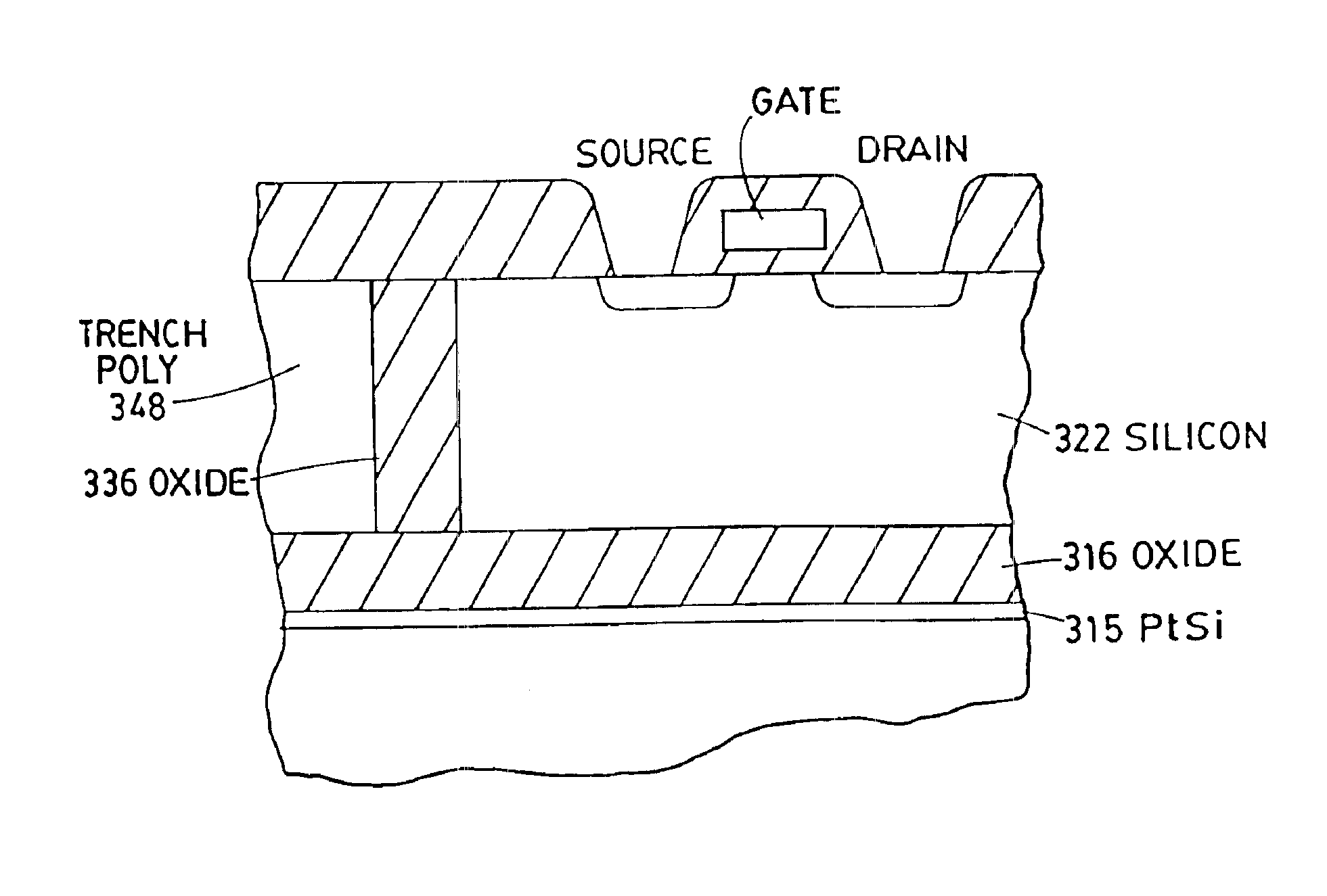
[0022](a) Begin with a four-inch diameter 500 μm-thick silicon device wafer 302 and a comparable diameter 500-μm thick silicon handle wafer 312. Device wafer 302 has the doping type and resistivity (e.g., N type and 20 ohm-cm resistivity) desired for eventual device fabrication. Thermally oxidize device wafer 302 to form oxide layer 316. Oxide 316 will become the bottom oxide, so the oxide is grown to the desired bottom oxide thickness, e.g., about 2-4 μm. Alternatively, diamond or silicon nitride (“nitride”) can be deposited on device wafer 302 to form the buried dielectric layer 316. A diamond thin film 316 can be deposited by a chemical vapor deposition (CVD) reaction of methane and hydrogen, and a nitride thin film can be deposited by decomposition of silane and ammonia.

[0023]Deposit a 500-angstrom thick polysilicon...


PUM


Abstract

A silicon-on-insulator integrated circuit comprises a handle die, a substantially continuous and unbroken silicide layer over the handle die, and a substantially continuous and unbroken first dielectric layer overlying one side of the silicide layer. A device silicon layer having an upper surface overlies the first dielectric layer, and a second dielectric layer on the handle die underlies the opposite side of the silicide layer. Interconnected transistors are disposed in and at the upper surface of the device silicon layer. A silicon-on insulator integrated circuit includes a handle die and a first dielectric layer formed on the handle die. A substantially continuous and unbroken silicide layer is formed on the first dielectric layer; the silicide layer has a controlled resistance and provides a diffusion barrier to impurities. A substantially continuous and unbroken second dielectric layer is disposed between the silicide layer and a device silicon layer, and trenches extend through the device silicon layer and silicide layer and separate the device silicon layer into islands, each having an underlying continuous silicide area. Interconnected transistors are disposed in and at an upper surface of the device silicon layer. A bonded wafer integrated circuit comprised a handle die and a homogeneous silicide layer bonded to the handle die. A device layer is bonded to the silicide layer, and interconnected transistors are disposed in and at a surface of device layer.

Description

CROSS-REFERENCE TO RELATED APPLICATIONS[0001]This application is a continuation of U.S. application Ser. No. 08 / 915,841, filed Aug. 21, 1997, now abandoned; which is a continuation of U.S. application Ser. No. 08 / 681,038, filed Jul. 22, 1996, now abandoned; which is a division of U.S. application Ser. No. 08 / 351,933, filed Dec. 8, 1994, now U.S. Pat. No. 5,569,620; which is a continuation of U.S. application Ser. No. 07 / 939,786, filed Sep. 3, 1992, now U.S. Pat. No. 5,387,555, the disclosures of which are incorporated herein by reference.[0002]This application is also a continuation of U.S. application Ser. No. 07 / 834,439, filed Feb. 12, 1992, now U.S. Pat. No. 5,266,135; U.S. application Ser. No. 07 / 921,197, filed Jul. 28, 1992, now U.S. Pat. No. 5,362,667; and U.S. application Ser. No. 08 / 430,312, filed Apr. 28, 1995, now U.S. Pat. No. 5,849,627, the disclosures of which are incorporated herein by reference.FIELD OF THE INVENTION[0003]The present invention relates to electronic in...

Claims


Application Information

Patent Timeline
Patent Type & Authority Patents(United States)
IPC IPC(8): H01L21/762H01L21/02H01L21/20H01L21/70H01L21/316
CPCH01L21/2007H01L21/31654H01L21/76264H01L21/76286H01L21/76275H01L21/76283H01L21/02233
Inventor LINN, JACK H.LOWRY, ROBERT K.ROUSE, GEORGE V.BULLER, JAMES F.
Owner INTERSIL CORP
Why Eureka
Try Eureka