Surface modification method

a surface modification and silicon oxide film technology, applied in the field of semiconductor device manufacture methods, can solve the problems of increasing the nitrogen concentration in the interface between silicon and silicon oxide film, nitriding silicon oxide film, not yet being reduced to practice, etc., to achieve rapid surface modification, increase the nitrogen concentration, and reduce the nitrogen concentration

Inactive Publication Date: 2005-07-12
CANON KK
View PDF5 Cites 6 Cited by
  • Summary
  • Abstract
  • Description
  • Claims
  • Application Information

AI Technical Summary

Benefits of technology

[0012]Accordingly, it is an exemplary object of the present invention to provide a surface modification method, which eliminates the above prior art disadvantages, and provides a rapid surface modification that generates by a less damaged, high-quality oxynitride film sufficiently reducing a nitrogen concentration at an interface between a silicon oxide film and a silicon substrate while increasing a nitrogen concentration in a silicon oxide film.

Problems solved by technology

Thus, a nitrogen concentration distribution in a depth direction in the silicon oxide film as a result of thermal nitriding does not locate nitrogen on a surface, and causes increased nitrogen concentration in the interface between silicon and the silicon oxide film.
These conventional methods for nitriding a silicon oxide film have several disadvantages and have not yet been reduced to practice.
For example, the heat nitriding process has a high nitrogen concentration at the interface of a silicon oxide film and silicon, and causes inferior device characteristics, such as low mobility of a channel in a transistor.
On the other hand, the remote plasma process cannot obtain sufficient nitrogen active species since necessary nitrogen active species decreased with the nitrogen ions in the plasma, and takes a very long process time.
In addition, this process cannot enhance the nitrogen surface density since the nitrogen concentration distribution in a depth direction in the silicon oxide film decreases drastically by depth.
The nitriding process using ions at low pressure and temperature leaves damages in a silicon thermal oxide film, deteriorates performance in leak current and boron dispersion prevention.
Damages recover at high temperature, but nitrogen disperses in a high temperature process and a shallow nitride layer cannot be obtained.

Method used


Image

  • Surface modification method
  • Surface modification method
  • Surface modification method

Examples


first embodiment

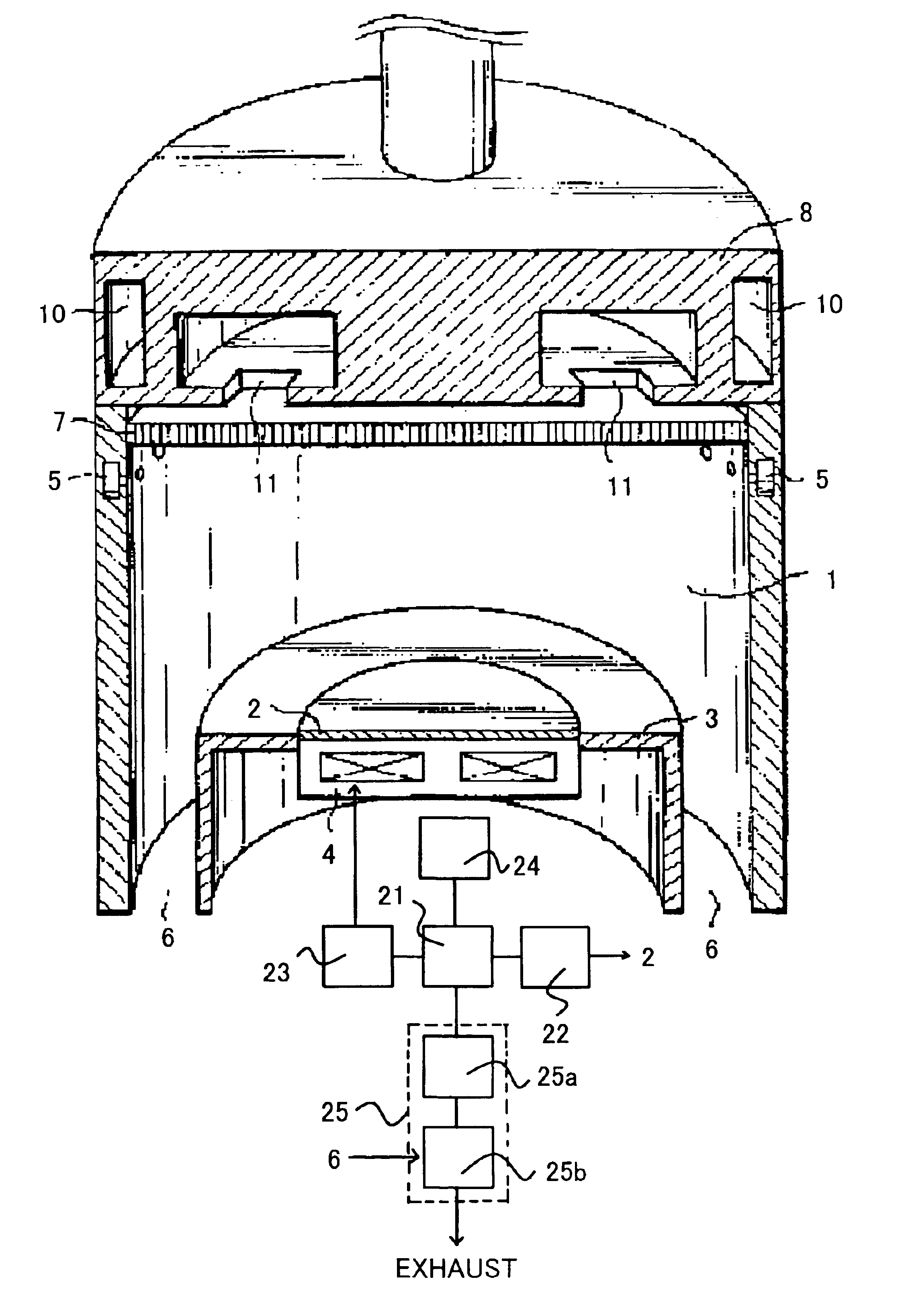
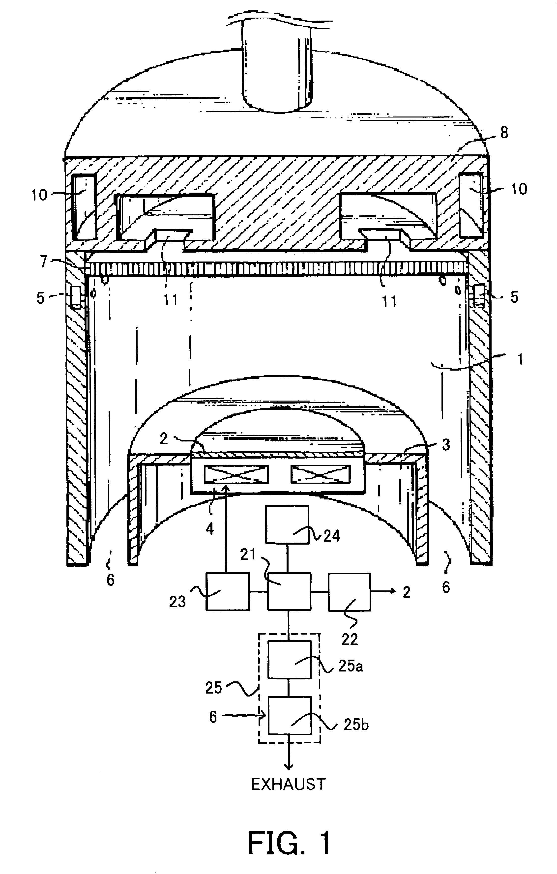
[0042]A description will now be given of a second embodiment according to the present invention, using a microwave surface-wave interference plasma processing apparatus shown in FIG. 1. First, the heater 4 heats the substrate stage 3 up to 200° C., and the substrate 2 that forms a silicon oxide film having a thickness of 2 nm on its surface is fed to and placed on the stage 3. Next, the plasma process chamber 1 is vacuum-exhausted by the exhaust system 25 down to 1 Pa. Then, nitrogen gas is introduced into the plasma process chamber 1 at 500 sccm through the process gas introducing means 5. Then, the pressure regulating valve 25a, such as a conductance valve, provided in the exhaust system 25 is regulated so as to hold the pressure in the plasma process chamber 1 to 133 Pa.

[0043]Then, the microwave power supply (not shown) supplies the plasma process chamber 1 with microwaves of 1.5 kW through the slot-cum non-terminal circle waveguide 8 and dielectric window 7, thereby generating p...

second embodiment

[0045]A description will now be given of a second embodiment according to the present invention, using a microwave surface-wave interference plasma processing apparatus shown in FIG. 1. First, the heater 4 heats the substrate stage 3 up to 200° C., and the substrate 2 that forms a silicon oxide film having a thickness of 2 nm on its surface is fed to and placed on the stage 3. Next, the plasma process chamber 1 is vacuum-exhausted by the exhaust system 25 down to 1 Pa. Then, nitrogen gas is introduced into the plasma process chamber 1 at 500 sccm through the process gas introducing means 5. Then, the pressure regulating valve 25a, such as a conductance valve, provided in the exhaust system 25 is regulated so as to hold the pressure in the plasma process chamber 1 to 26.6 Pa.

[0046]Then, the microwave power supply (not shown) supplies the plasma process chamber 1 with microwaves of 1.5 kW through the slot-cum non-terminal circle waveguide 8 and dielectric window 7, thereby generating ...

third embodiment

[0048]A description will now be given of a third embodiment according to the present invention, using a microwave surface-wave interference plasma processing apparatus shown in FIG. 1. The instant embodiment has an object to provide an effective and quick nitride process by adding inert gas to gas that contains nitrogen, and raising the plasma density by 2 to 3 times.

[0049]The plasma process is conducted using microwave surface-wave interference plasma processing apparatus shown in FIG. 1 as follows: First, the heater 4 heats the substrate stage 3 up to 150° C., and the substrate 2 that forms a silicon oxide film having a thickness of 2 nm on its surface is fed to and placed on the stage 3. Next, the plasma process chamber 1 is vacuum-exhausted by the exhaust system 25 down to 1 Pa. Then, nitrogen gas of 50 sccm and argon of 450 sccm are introduced into the plasma process chamber 1 through the process gas introducing means 5. Then, the pressure regulating valve 25a, such as a conduc...


PUM

PropertyMeasurementUnit
temperatureaaaaaaaaaa
pressureaaaaaaaaaa
temperatureaaaaaaaaaa

Abstract

A method for modifying a surface of a substrate to be processed, by utilizing plasma includes the steps of adjusting a temperature of the substrate from 200° C. to 400° C., introducing gas including nitrogen atoms or mixture gas including inert gas and the gas including nitrogen atoms into a plasma process chamber, adjusting pressure in the plasma process chamber above 13.3 Pa, generating plasma in the plasma process chamber, and injecting ions equal to or smaller than 10 eV in the plasma into the substrate to be processed.

Description

[0001]This application claims a benefit of priority based on Japanese Patent Application No. 2002-343855, filed on Nov. 27, 2002, which is hereby incorporated by reference herein in its entirety as if fully set forth herein.BACKGROUND OF THE INVENTION[0002]The present invention relates generally to semiconductor manufacture methods, and more particularly to a method that provides high-quality and quick modification to a substrate to be processed, by utilizing microwave surface-wave plasma. The present invention is suitable, for example, for a method for forming a silicon oxynitride film.[0003]Along with recent fine processing of semiconductor devices, a silicon oxynitride film has been applied in a gate insulating film with a thickness below 3 nm. A silicon oxynitride film is made by introducing nitrogen into a silicon oxide film. The silicon oxynitride film has attracted attention due to its excellent characteristics such as high specific permittivity, leak current prevention, and ...

Claims


Application Information

Patent Timeline
Patent Type & Authority Patents(United States)
IPC IPC(8): H01J37/32H01L21/28H01L21/02H01L21/314C08J7/00H01L29/51
CPCH01J37/32192H01L21/28194H01L29/518H01L21/3144H01L21/28202H01L21/0234H01L21/02332
Inventor KITAGAWA, HIDEOSUZUKI, NOBUMASAUCHIYAMA, SHINZO
Owner CANON KK
Why Eureka
Try Eureka