

High temperature superconducting thick films
a superconducting, high-temperature technology, applied in the direction of superconducting magnets/coils, magnetic bodies, natural mineral layered products, etc., can solve the problem that the ysz layer was considered too slow for commercial production
- Summary
- Abstract
- Description
- Claims
- Application Information
AI Technical Summary
Benefits of technology
Problems solved by technology
Method used
Image

Examples
example 1
[0034]An ion-assisted, electron beam evaporation system similar to that of Wang et al., App. Phys. Lett., v. 71, no. 20, pp. 2955-2957 (1997), was used to deposit a MgO film upon a flexible metal substrate of Hastelloy C-276 or other nickel-based alloys. The substrates were ultrasonically cleaned in soap and water, rinsed with deionized water, rinsed with methanol and blown dry with filtered nitrogen. The ion source was manufactured by Ion Tech, Inc. (Ft. Collins, Colo.) with a source geometry of 22 cm by 2.5 cm. The substrate normal to ion-assist beam angle was 45±3°. The ion source gas was argon. The ion source gas was introduced to a background partial pressure of about 1.0×10⁻⁶ Torr with a total pressure during deposition of about 1×10⁻⁴ Torr. The electron gun heated the MgO source to maintain a deposition rate of about 0.15 nm / sec. The ion-assist gun voltage and current density were about 750 eV and 100 μA / cm2 respectively.
[0035]Various amorphous oxide materials were used and x...
example 2
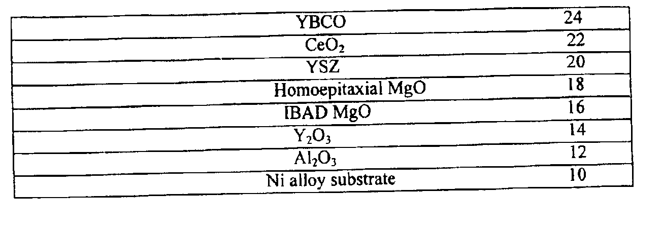
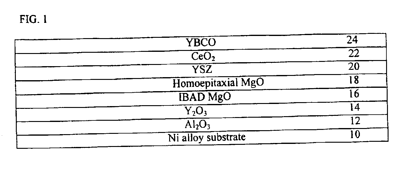
[0037]On a nickel alloy substrate (Hastelloy C276), was deposited by magnetron sputter deposition a layer of aluminum oxide about 800 to about 1000 Angstroms in thickness. The aluminum oxide layer was then polished by CMP (chemical-mechanical-polishing) with a colloidal suspension of silica as the polishing medium. The resultant surface of the aluminum oxide had a smoothness (RMS roughness) of about 1 nm. Onto this resultant article was deposited a layer of Y2O3 (about 5 nm) by e-beam evaporation. Onto this resultant article was deposited a layer of MgO about 10 nm in thickness using ion beam assisted electron beam deposition with an ion assist gas of argon. Onto the IBAD-MgO layer was then deposited a layer of homoepitaxial MgO by e-beam evaporation. Onto the top MgO layer was deposited a layer of yttria-stabilized zirconium (YSZ) about 30 nm in thickness by pulsed laser deposition. Onto the layer of YSZ was deposited a layer of cerium oxide about 30 nm in thickness by pulsed laser...
example 3
[0038]On a nickel alloy substrate (Haynes 242), was deposited by magnetron sputter deposition a layer of aluminum oxide about 80 nm to 100 nm in thickness. The aluminum oxide layer was then polished by CMP (chemical-mechanical polishing) with a colloidal suspension of silica as the polishing medium. The resultant surface of the aluminum oxide had a smoothness (RMS roughness) of 1 nm. Onto this resultant article was deposited a layer of AlON (about 20 nm) by magnetron sputter deposition. Onto this resultant article was deposited a layer of MgO about 10 nm in thickness using ion beam assisted electron beam deposition with an ion assist gas of argon. Onto the IBAD-MgO layer was then deposited a layer of homoepitaxial MgO by e-beam evaporation. Onto the top MgO layer was deposited a layer of yttria-stabilized zirconium (YSZ) about 30 nm in thickness by pulsed laser deposition. Onto the layer of YSZ was deposited a layer of cerium oxide about 30 nm in thickness by pulsed laser deposition...
PUM
| Property | Measurement | Unit |
|---|---|---|
| RMS roughness | aaaaa | aaaaa |
| thickness | aaaaa | aaaaa |
| temperatures | aaaaa | aaaaa |
Abstract
Description
Claims
Application Information