System and method for fabricating efficient semiconductor lasers via use of precursors having a direct bond between a group III atom and a nitrogen atom

a technology of precursors and semiconductor lasers, applied in the direction of semiconductor lasers, lasers, coatings, etc., can solve the problems of limiting the amount of data that may be transmitted via traditional communication lines, traditional communication lines are susceptible to interference, and many disadvantages, and achieve high sticking coefficient, high n incorporation in ingaasn, and large supply of precursors

Inactive Publication Date: 2005-08-23
AVAGO TECH WIRELESS IP SINGAPORE PTE
View PDF10 Cites 10 Cited by
  • Summary
  • Abstract
  • Description
  • Claims
  • Application Information

AI Technical Summary

Benefits of technology

[0017]Due to the present nitrogen precursor having a group III-N direct bond, the nitrogen precursor has a high sticking coefficient and therefore, a large supply of N precursor is not necessary to obtain a relatively high N incorporation in InGaAsN. In addition, by using the present nitrogen precursors, InGaAsN can be grown under higher growth temperature and a high As / group III ratio, which typically enables growth of high quality GaAs-based materials. Further, there is less possibility that impurities will be incorporated into InGaAsN layers due to low N precursor supply. The high sticking coefficient of the present N precursors also equates to ease in obtaining higher N composition in InGaAsN with a higher mole fraction of In.

Problems solved by technology

Traditional communication lines, such as cable containing copper wire, have been used to cater to this continuously growing demand, however, traditional communication lines are subject to many disadvantages.
Traditional communication lines are susceptible to interference during the transmission of data.
Traditional communication lines are also characterized by a limited bandwidth, thereby limiting the amount of data that may be transmitted via traditional communication lines.
However, it is difficult to grow high quality distributed Bragg reflectors (DBRs) of a vertical cavity surface-emitting laser (VCSEL) using InGaAsP material.
However, using InGaAsN in a semiconductor gives rise to significant manufacturing challenges.
There are, however, negative aspects associated with the use of DMHy as a nitrogen precursor.
However, due to extremely low N incorporation in InGaAsN by MOCVD with DMHy as the N precursor, a ratio of more than 95% DMHy / total group-V precursor ratio is supplied to an MOCVD reactor to obtain 1% N / total group-V atoms in solid composition, resulting in large consumption of DMHy.
In addition, the following InGaAsN quality issues result from use of DMHy as a nitrogen precursor.
Unfortunately, a low As / group III ratio typically causes poor material quality in GaAs based semiconductors.
Another negative aspect associated with the use of DMHy as a nitrogen precursor is that the purity of DMHy is currently difficult to control, especially for residual water level.
Water contamination in DMHy causes poor material quality of semiconductors.
Therefore, it is difficult to obtain 1.55 μm emission from InGaAsN, which should have 40% In and 3% N, by MOCVD growth and with using DMHy as a N precursor.

Method used


Image

  • System and method for fabricating efficient semiconductor lasers via use of precursors having a direct bond between a group III atom and a nitrogen atom
  • System and method for fabricating efficient semiconductor lasers via use of precursors having a direct bond between a group III atom and a nitrogen atom
  • System and method for fabricating efficient semiconductor lasers via use of precursors having a direct bond between a group III atom and a nitrogen atom

Examples


Embodiment Construction

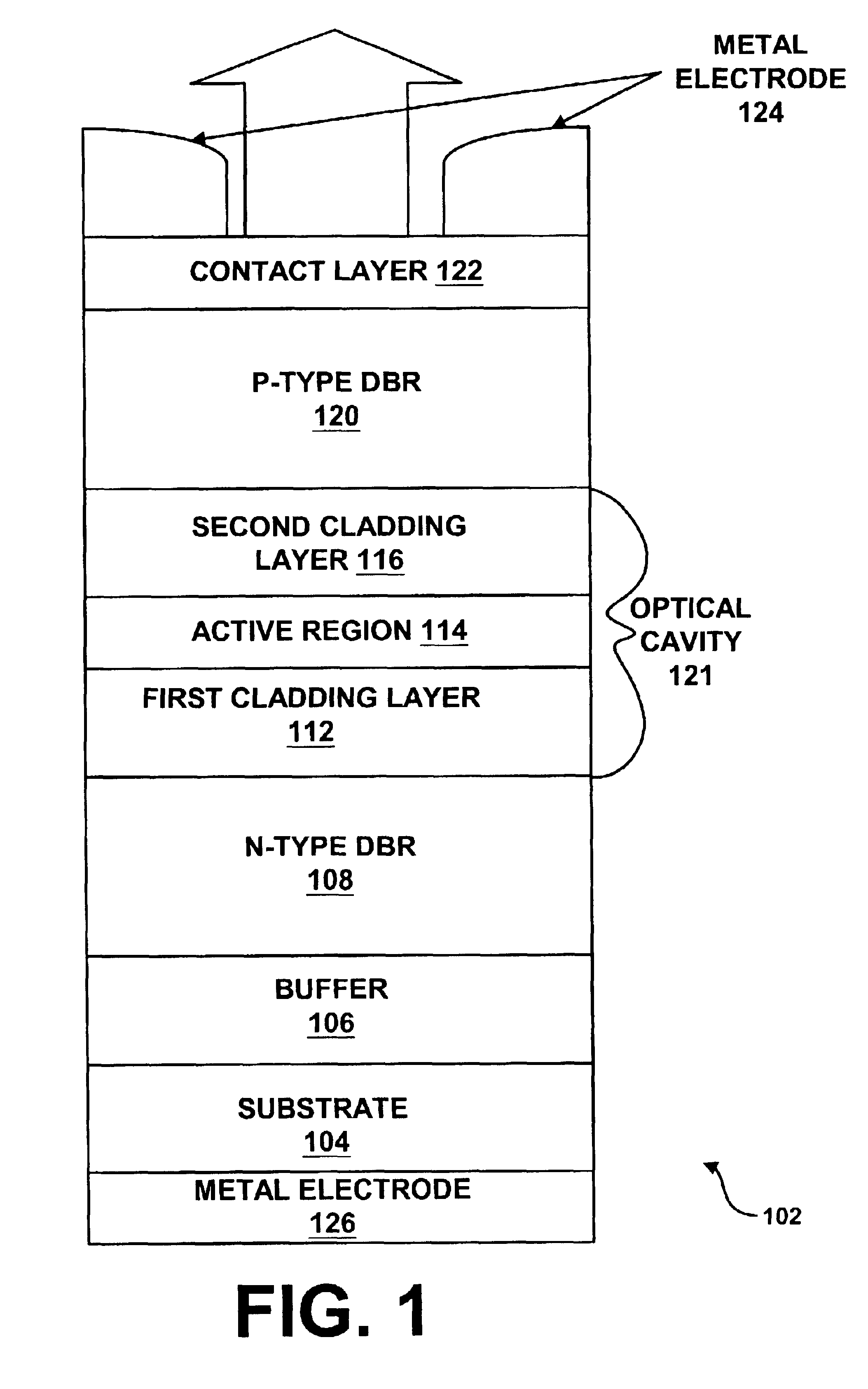
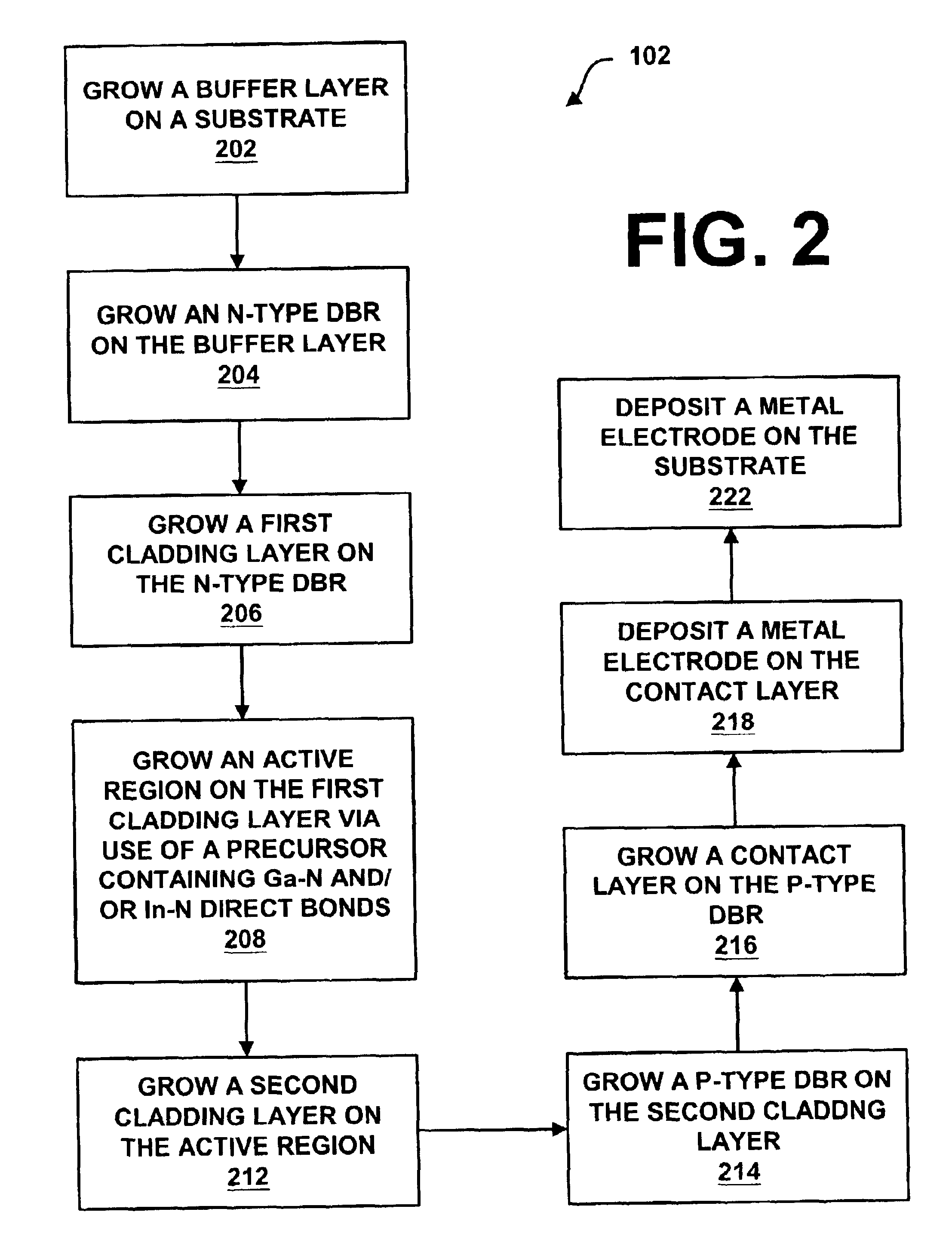
[0026]While the present description and embodiments provided herein refer to a semiconductor laser fabrication system and method, it should be noted that the present system and method may be utilized for other light emitting devices, such as a light emitting diode (LED).

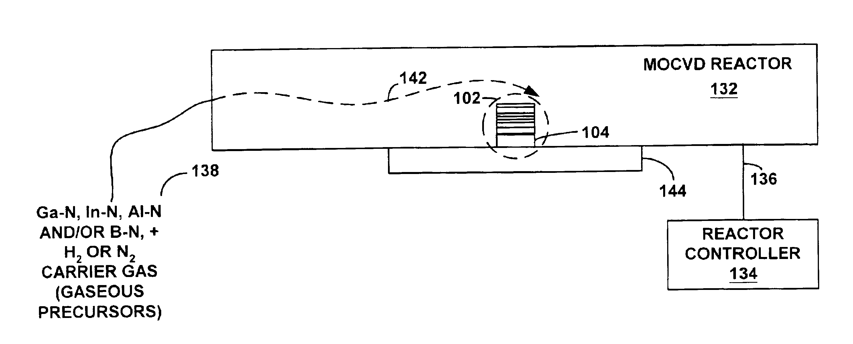
[0027]The semiconductor laser fabrication system and method use a nitrogen precursor having a direct bond between a group III atom and a nitrogen atom to fabricate an InGaAsN layer. InGaAsN is an attractive material used in semiconductor lasers since InGaAsN can be grown on GaAs wafers. The use of InGaAsN results in a higher conduction band offset and enables highly reflective GaAs / AlAs distributed Bragg reflectors to be used. In addition, a semiconductor laser having InGaAsN in its active region can produce light having relatively long wavelength, in the range of approximately 1.2-1.6 μm. Light in this wavelength range is transmitted by an optical fiber with relatively little loss of light intensity over long distan...


PUM

PropertyMeasurementUnit
wavelengthaaaaaaaaaa
wavelength in the rangeaaaaaaaaaa
decomposition temperatureaaaaaaaaaa

Abstract

A system for fabricating a light emitting device is disclosed. The system contains a growth chamber and at least one nitrogen precursor that is introduced to the growth chamber. The at least one nitrogen precursor has a direct bond between at least one group III atom and at least one nitrogen atom. In addition, the nitrogen precursor is used to fabricate a layer constituting part of an active region of the light emitting device containing indium, gallium, arsenic, and nitrogen, wherein the active region produces light having a wavelength in the range of approximately 1.2 to 1.6 micrometers. A method for fabricating a semiconductor structure is also disclosed. The method comprises providing a substrate and growing over the substrate a layer comprising indium, gallium, arsenic, and nitrogen using at least one nitrogen precursor having a direct bond between at least one group III atom and at least one nitrogen atom.

Description

FIELD OF THE INVENTION[0001]The present invention generally relates to semiconductor devices and, more particularly, is related to semiconductor laser fabrication.BACKGROUND OF THE INVENTION[0002]With advances in technology, there is a continuous demand to increase data transmission rates and volume of data transmission. Traditional communication lines, such as cable containing copper wire, have been used to cater to this continuously growing demand, however, traditional communication lines are subject to many disadvantages. Traditional communication lines are susceptible to interference during the transmission of data. Examples of such interference include, but are not limited to, electromagnetic interference and inter-symbol interference. Traditional communication lines are also characterized by a limited bandwidth, thereby limiting the amount of data that may be transmitted via traditional communication lines.[0003]Fiber-optic telecommunication systems have been introduced to the...

Claims


Application Information

Patent Timeline
Patent Type & Authority Patents(United States)
IPC IPC(8): H01S5/323H01S5/00H01L21/205C23C16/34H01S5/183
CPCH01S5/32341H01L21/02395H01L21/02458H01L21/02461H01L21/02463H01L21/02507H01L21/02546H01L21/02576H01L21/0262H01S2304/025
Inventor TAKEUCHI, TETSUYATAN, MICHAELCHANG, YING-IAN
Owner AVAGO TECH WIRELESS IP SINGAPORE PTE
Why Eureka
Try Eureka