Microstructure apparatus and method for separating differently charged molecules using an applied electric field

a microstructure apparatus and electric field technology, applied in the field of microstructure apparatus, can solve the problems of high quantity of sup>32/sup>p to be used in assays, difficult to eliminate waste, and difficult to use, etc., to achieve the effect of simplifying device design and construction

Inactive Publication Date: 2005-09-13
NANOGEN INC
View PDF31 Cites 22 Cited by
  • Summary
  • Abstract
  • Description
  • Claims
  • Application Information

AI Technical Summary

Benefits of technology

[0010]The devices and methods of the present invention provide a simple solution to the problem of separating differently charged molecules in a sample for the detection of a molecule of interest. These methods and devices are particularly suitable for analyzing substrate-enzyme reactions, or other simple biochemical model systems where a labeled molecule may undergo change in net charge, in a highly parallel manner. The devices of the invention utilize a capture matrix located in the

Problems solved by technology

The use of 32P in assays, however, poses significant disadvantages.
One major problem is that, for sensitive detection, relatively high quantities of 32P must be used routinely and subsequently disposed.
Due to government restrictions, this waste cannot be disposed of easily.
Another disadvantage is the hazard posed to personnel working with the

Method used


Image

  • Microstructure apparatus and method for separating differently charged molecules using an applied electric field
  • Microstructure apparatus and method for separating differently charged molecules using an applied electric field
  • Microstructure apparatus and method for separating differently charged molecules using an applied electric field

Examples


example 1

Electrophoretic Planar Microstructures Formed in PDMS

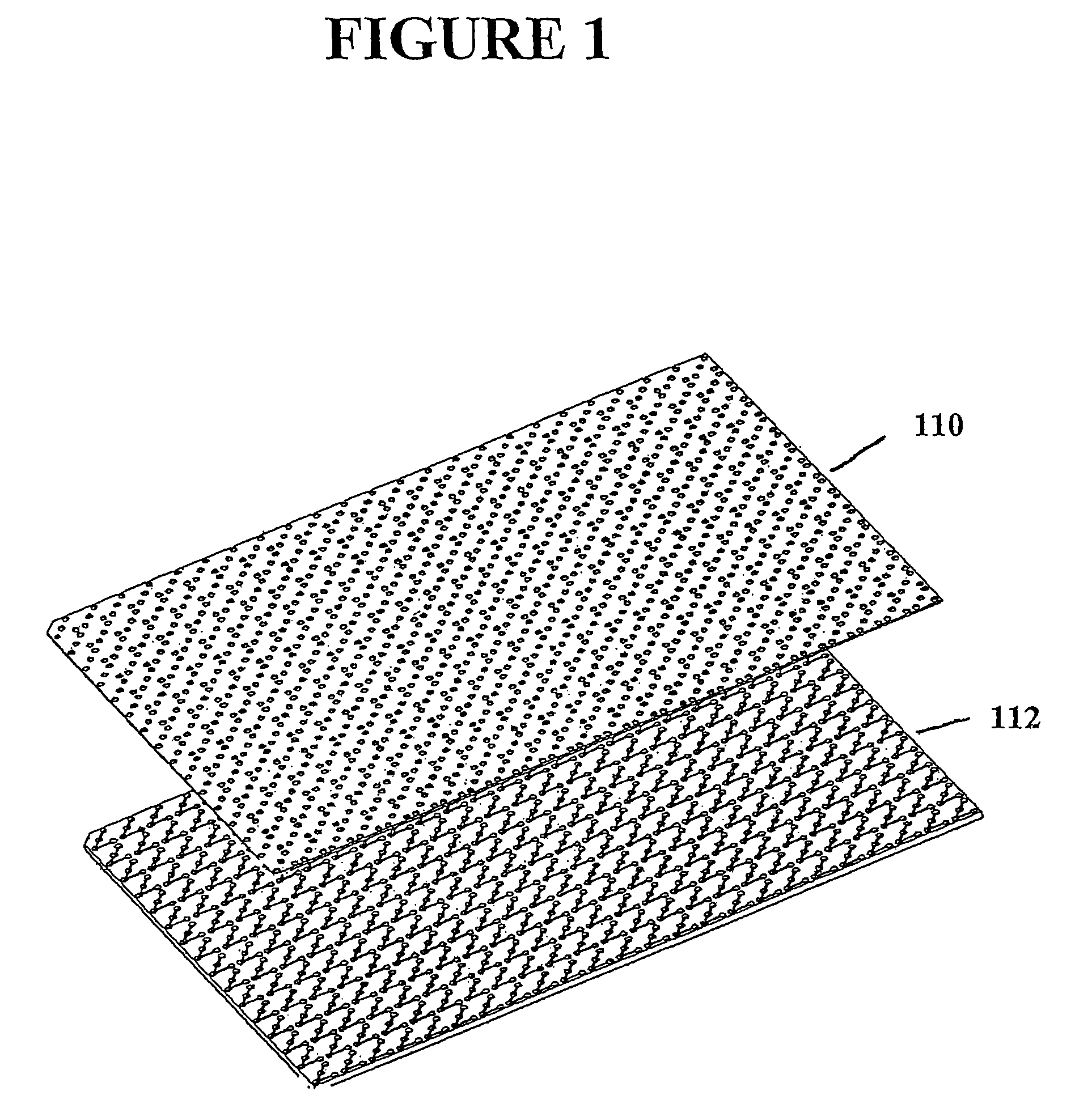
[0069]Microfluidic structures were fabricated using SU-8 photoresist and poly(dimethylsiloxane) (PDMS). 384 single capture format microstructures with port size of 1 mm and channel size of 250 μm were designed in an 8.5X11 cm footprint similar to microtiter plates, as shown in FIG. 1. This design was converted into a transparency by a high-resolution printer. The transparency was used as a mask in photolithography to create a master in SU-8 photoresist. PDMS cast against the master yielded a polymeric replica containing 384 of the desired microstructures. The surface of this replica was then oxidized in oxygen plasma. Oxidation of the PDMS yields channels whose walls are negatively charged when in contact with neutral and basic aqueous solutions. These channels have the advantage of being filled easily, even with liquids with high surface energies (especially water). As shown in FIG. 4b, fairly clean channels and microstructure se...

example 2

Use of the PDMS Planar Structures to Separate Kinase Products from Substrates

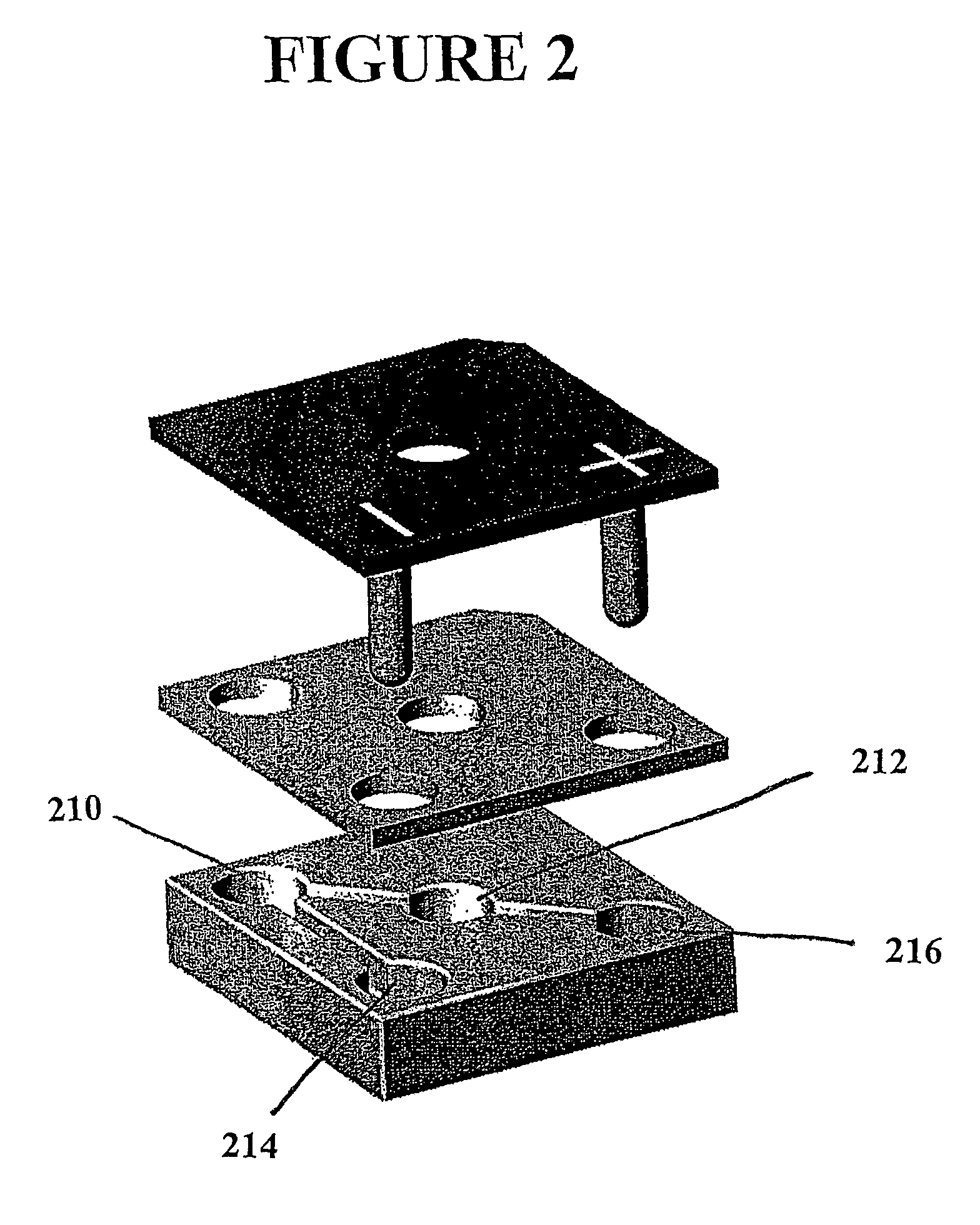
[0070]Each microstructure used in these experiments was composed of 4 ports and three channels, as depicted in FIG. 4b. In general, the sample (a peptide substrate mixture which has been reacted with a kinase enzyme) is introduced through an opening in the sealing plate into the sample chamber (S). The electrode assembly is then energized, biasing the (+) and (−) chambers positive and negative, respectively. Negatively charged components of the sample migrate toward the positive electrode and into the capture port (C). This port contains a matrix (Biodyne B, Pall Inc.) that irreversibly binds peptide and is located in the center of the structure to allow fluorescence detection with a standard plate reader.

[0071]Kemptide discrimination assays were performed in PDMS structures fabricated as described in Example 1. A 0.9 mm diameter Biodyne B membrane disc was inserted into the capture port. The structure was ...

example 3

3D Electrophoretic Microstructures

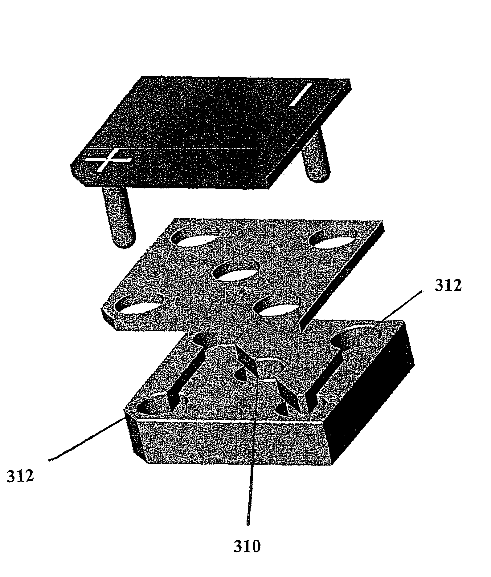
[0072]The microstructures described in example 1 could be modified to have several more layers, creating a three dimensional channel microstructure. When an electric field is applied across these structures, the molecules of interest may travel orthogonally through the capture matrix to bind, rather than travelling tangentially across the capture matrix. Tangential-flow arrangements generally produce moon-shaped deposits on the capture matrix, as shown in FIG. 5c. Using and orthogonal flow approach may increase the uniformity and reproducibility of the signal on the capture matrix. A depiction of a three-dimensional channel and chamber microstructure is shown in FIG. 9.

[0073]One approach to making three-dimensional layered structures is to use several layers of perforated and formed polymer material. As illustrated in FIG. 10, a bottom polymer layer may be used which has molded channels and microstructure sections forming a portion of the microstruc...


PUM


Abstract

The field of the present invention relates generally to a microstructure apparatus which may be used in a high-throughput screening context to monitor the rate of reaction of an enzyme with its substrate in cases where the product of the reaction has an altered net charge. For example, the systems and methods disclosed herein may be used to detect the activity of phosphatase enzymes, proteases and kinases on charged peptide substrates. The microstructure devices of the present invention comprise a plurality of microstructures, wherein each microstructure comprises a capture matrix located between two electrodes.

Description

FIELD OF INVENTION[0001]The field of the present invention relates generally to a microstructure apparatus which may be used in a high-throughput screening context to monitor the rate of reaction of an enzyme with its substrate in cases where the product of the reaction has an altered net charge. For example, the systems and methods disclosed herein may be used to detect the activity of phosphatase enzymes, proteases and kinases on charged peptide substrates. The microstructure devices of the present invention comprise a plurality of microstructures, wherein each microstructure comprises a capture matrix located between two electrodes.BACKGROUND OF THE INVENTION[0002]Protein kinases are of particular interest in drug discovery research because they have been shown to be key regulators of many cell functions, including signal transduction (Ullrich and Schlessinger, 1990), transcriptional regulation (Pawson and Bernstein, 1990), cell motility (Miglietta and Nelson, 1988) and cell divi...

Claims


Application Information

Patent Timeline
IPC IPC(8): B01D57/02G01N27/447B01L3/00
CPCB01D57/02G01N27/44717G01N27/44726G01N27/44747G01N27/44782B01L3/5027
Inventor JALALI, SHILAHARPER, ALANSIMPSON, MATTSWANSON, PAULHAVENS, JOHN
Owner NANOGEN INC
Why Eureka
Try Eureka