Transmission line and semiconductor integrated circuit device

a technology of integrated circuits and transmission lines, which is applied in the direction of waveguide devices, multi-port networks, waveguide type devices, etc., can solve the problems of large voltage drop of power voltage supplied from the bias terminal tvd, unsatisfactory high frequency isolation characteristics between the elements and between the terminals both connected by transmission lines,

Inactive Publication Date: 2005-09-20
PANASONIC CORP
View PDF8 Cites 1 Cited by
  • Summary
  • Abstract
  • Description
  • Claims
  • Application Information

AI Technical Summary

Benefits of technology

[0107]Hereinafter, Examples that achieve advantageous effects of the transmission line of this embodiment by effectively changing the capacitance Cadd and the resistance Radd based on the principle of the present invention explained in the first embodiment will be described.
[0108]As Example 3 according to the second embodiment, a transmission line with the signal strip 3 and the resistive layer 4, wherein a width of the signal strip 3 was changed to 50 μm and a width of the resistive layer 4 was changed to 100 μm, was fabricated. The distance between the signal strip 3 and the resistive layer 4 was set to 15 μm. Other conditions were the same as those of Example 2.
[0109]FIG. 8 is a graph showing a frequency dependence of a transmission loss of the transmission line of Example 3. The vertical axis of FIG. 8 indicates an effective loss occurring in the transmission line when a high frequency signal passes therethrough, the effective loss being a value obtained by multiplying a maximum available power gain by −1.
[0110]As shown in FIG. 8, the transmission losses per 5 mm of the transmission line of Example 3 at 1 GHz, 5 GHz, and 10 GHz were 2.1 dB, 15.2 dB, and 29.2 dB, respectively. Here, the transmission loss at 1 GHz was increased because capacitance generated between the signal strip 3 and the resistive layer 4 was increased due to the increase in the width of the signal strip 3, whereby the effect of the present invention is exerted also on the low frequency signal. In turn, the transmission loss at 10 GHz was slightly reduced as compared with

Problems solved by technology

However, many problems are left unsolved with the conventional transmission lines and the communication apparatuses having the transmission lines.
Therefore, there has been a problem that high frequency isolation characteristics between the elements and between the terminals both connected by way of the transmission line are not satisfactory.
However, in the structure of FIG. 24, it is necessary to set the electric resistance of the resister 119 to a large value for the purpose of eliminating the low frequency component, and, with such large electric resistance, a voltage drop of the power voltage supplied from the bias terminal Tvd is large.
That is to say, a reduction in driving voltage of the MMIC may entail a drawback of deteriorating an amplifying efficiency in the MMIC and the like.
However, in the high frequency amplifier shown in FIG. 25, it is necessary to provide additionally the bypass condenser 122 having a capacitance value sufficient for short-circuiting the high frequency signal of intermediate frequency and the resister 121 in the high frequency amplifier shown in FIG. 23, thereby undesirably increasing a circuit area in the whole module.
The above described drawbacks exist in the semiconductor integrated circuit device other than the amplifier, such as a mixer, a frequency multiplier, a switch, an attenuator, a frequency demultiplier, and an orthogonal modulator.

Method used


Image

  • Transmission line and semiconductor integrated circuit device
  • Transmission line and semiconductor integrated circuit device
  • Transmission line and semiconductor integrated circuit device

Examples


first embodiment

(First Embodiment)

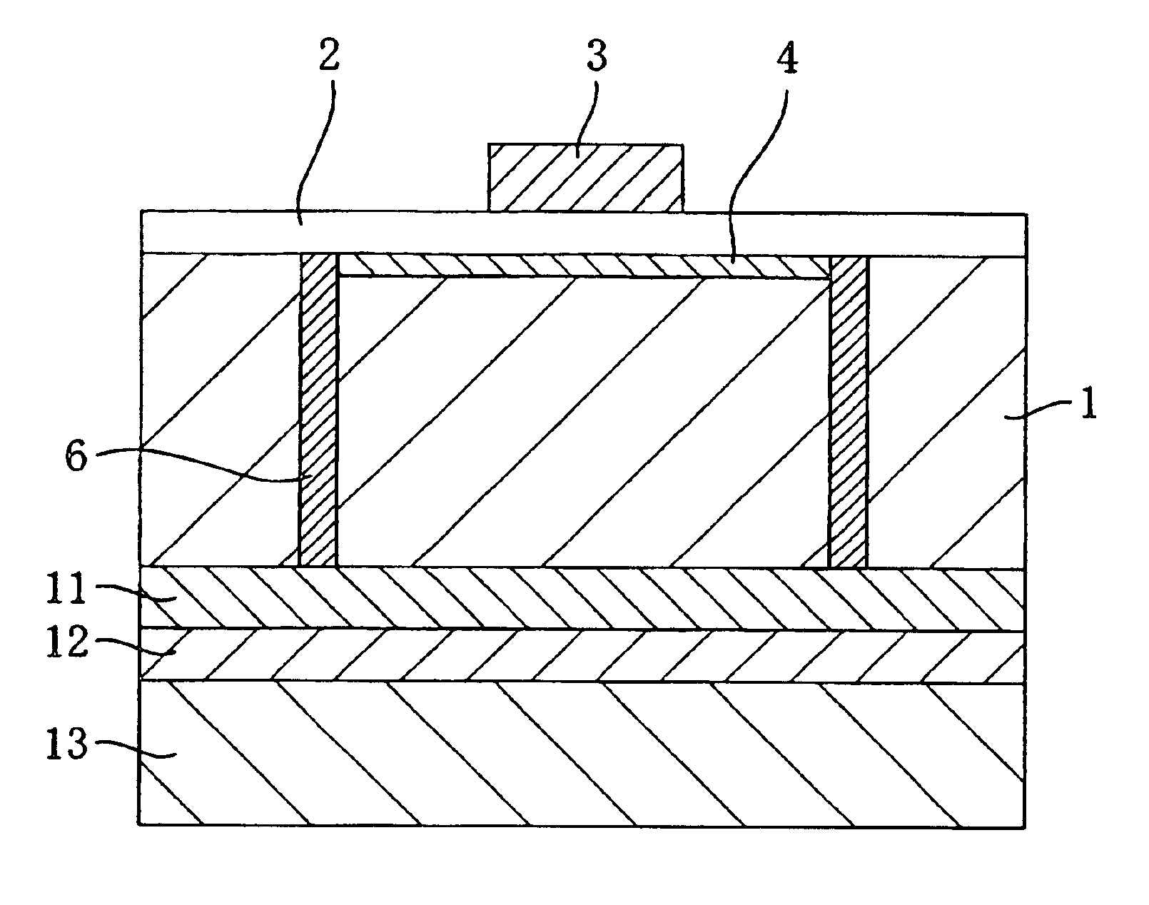
[0074]FIG. 1 is a sectional view showing a structure of a transmission line according to the first embodiment of the present invention, and FIG. 2 is a top view showing a structure of the transmission line of FIG. 1 as viewed from above.

[0075]As shown in FIG. 1, the transmission line of this embodiment is provided with a dielectric substrate 1, a dielectric film 2 disposed on a top face of the dielectric substrate 1, a signal strip 3 disposed on a top face of the dielectric film 2, a resistive layer 4 formed between the dielectric substrate 1 and the dielectric film 2 as opposed to the signal strip 3 with the dielectric film 2 disposed between the resistive layer 4 and the signal strip 3, a ground conductor layer 11 disposed on a bottom face of the dielectric film 2, penetrating conductors 6 penetrating the dielectric layer 2 to connect the resistive layer 4 to the ground conductor layer 11.

[0076]As shown in FIG. 2, the signal strip 3 and the resistive layer 4 are ...

example 1

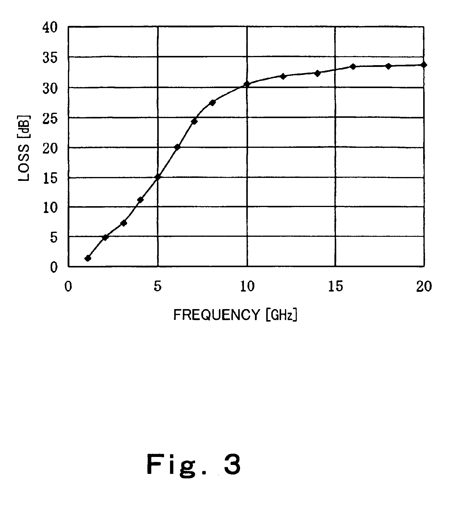
[0087]The transmission line having the structure shown in FIG. 1 was fabricated as Example 1 according to the first embodiment of the present invention under the following conditions. The dielectric substrate 1 was formed by a gallium arsenide (GaAs) substrate having a thickness of 500 μm and a dielectric constant of 13; the dielectric film 2 was formed by a silicon nitride (SiN) film having a thickness of 1 μm and a dielectric constant of 7; and the signal strip 3 and the ground conductor layer 5 were formed by gold having conductivity of 3×10⁷ S / m and a thickness of 5 μm. An impurity diffusion layer having a thickness of 0.2 μm and conductivity of 4×10⁴ S / m was formed directly under a surface of the dielectric substrate 1 formed from gallium arsenide, and the impurity diffusion layer was used as the resistive layer 4. A width of the signal strip 3 was 20 μm, and a width of the resistive layer 4 was 100 μm. The signal strip 3 and the resistive layer 4 were disposed in such a fashio...

second embodiment

(Second Embodiment)

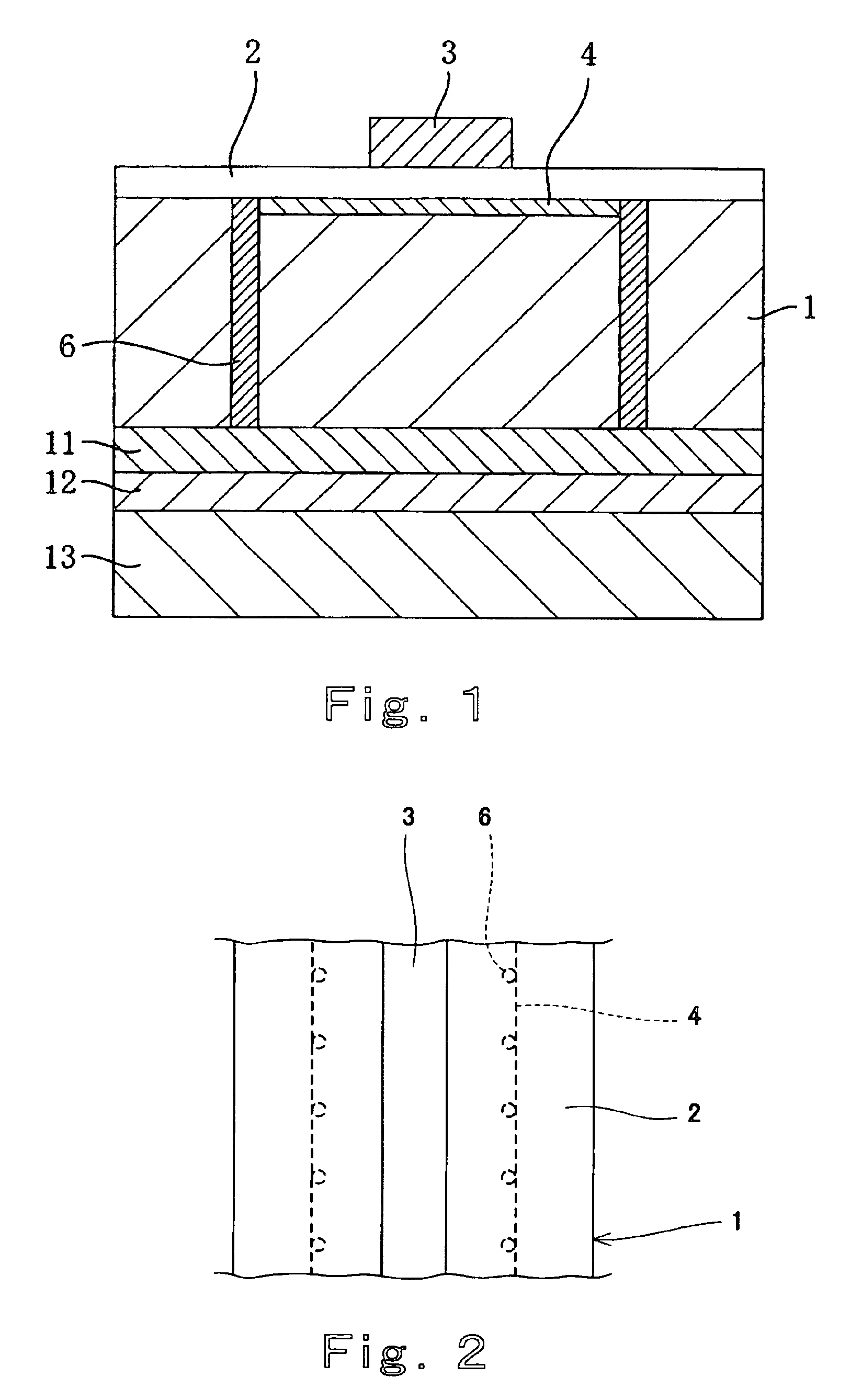
[0097]FIG. 5 is a sectional view schematically showing a structure of a transmission line according to the second embodiment of the present invention, and FIG. 6 is a top view showing a structure of the transmission line of FIG. 5 as viewed from above.

[0098]As shown in FIG. 5, the transmission line of this embodiment has a dielectric substrate 1, a dielectric film 2 disposed on a top face of the dielectric substrate 1, a signal strip 3 disposed on a top face of the dielectric film 2, a resistive layer 4 disposed between the dielectric substrate 1 and the dielectric film 2 as opposed to the signal strip 3 with the dielectric film 2 disposed between the resistive layer 4 and the signal strip 3, a pair of ground conductor layers 5 disposed on the top face of the dielectric film 2 as each opposed to the signal strip 3 with a predetermined spacing in the width direction of the signal strip 3, and penetrating conductors 6 penetrating the dielectric film 2 and connecting...


PUM


Abstract

The transmission line is provided with a signal strip, a resistive layer opposed to the signal strip across a dielectric layer, and a ground conductor electrically connected to the resistive layer, wherein, in the case where resistance per unit length occurring when a high frequency current induced in the resistive layer through capacitance formed by the dielectric layer between the signal strip and the resistive layer flows in the resistive layer and between the resistive layer and the ground conductor at the time of transmission of a high frequency signal of a predetermine frequency through the signal strip is defined as additional resistance and resistance per unit length occurring when the high frequency current flows through the ground conductor is defined as ground resistance, the additional resistance is larger than the ground resistance.

Description

[0001]This is a continuation application under 35 U.S.C 111(a) of pending prior International Application No. PCT / JP03 / 09784, filed on Aug. 1, 2003.BACKGROUND OF THE INVENTION[0002]1. Field of the Invention[0003]The present invention relates to a transmission line for handling high frequency signals in a microwave band, a millimeter wave band and the like and a semiconductor integrated circuit device having the transmission line.[0004]2. Description of the Related Art[0005]In a conventional communication apparatus using high frequency signals in a microwave band, a millimeter wave band, and the like as carrier waves, a transmission line such as a microstrip and a coplanar waveguide has generally been used as a bias supplying circuit for supplying power to an active device.[0006]FIGS. 22A and 22B are schematic sectional views respectively showing a structure of an ordinary microstrip and a structure of an ordinary coplanar waveguide.[0007]As shown in FIG. 22A, the microstrip has a di...

Claims


Application Information

Patent Timeline
Patent Type & Authority Patents(United States)
IPC IPC(8): H01L27/08H01P3/08H01P3/00H01L27/04H01L21/768H01L21/822H01L23/522H01L23/66H01P1/212H01P3/02H03F3/60
CPCH01L23/66H01L27/0802H01L27/0805H01P3/003H01P3/081H01L2223/6627H01L2924/1903H01L2924/3011H01L2924/0002H01L2924/00
Inventor KANNO, HIROSHI
Owner PANASONIC CORP
Why Eureka
Try Eureka