
Method and apparatus for forming thin film of metal

a thin metal film and metal technology, applied in the direction of solid-state diffusion coating, liquid/solution decomposition chemical coating, conductive pattern formation, etc., can solve the problem of not being able to actually form patterns on metals that are difficult to etch, need an increased number of steps, and increase the number of steps. , to achieve the effect of increasing product quality and increasing yield

Inactive Publication Date: 2005-12-06
EBARA CORP
View PDF7 Cites 19 Cited by
  • Summary
  • Abstract
  • Description
  • Claims
  • Application Information

AI Technical Summary

Benefits of technology

This approach enables the efficient and stable formation of high-quality thin metal films, improving conductivity and reducing environmental impact by eliminating the need for etching or plating, while allowing for precise control over film thickness and uniformity.

Problems solved by technology

However, the process of forming a pattern according to etching, for example, needs an increased number of steps, and fails to actually form patterns on metals that are difficult to etch.
While the plating processes are an inexpensive and highly technically accomplished technology, the electrolytic plating process is capable of growing a film only on an electrically conductive material, whereas the electroless plating process suffers a problem in that substances contained in the plating liquid affect the natural environment and the working environment.

Method used


Image

  • Method and apparatus for forming thin film of metal
  • Method and apparatus for forming thin film of metal
  • Method and apparatus for forming thin film of metal

Examples


example 1

[0103]Oleic acid was used as an organic anionic substance, and silver acetate was used as a metal source. 0.5 L of a naphthene-based high boiling solvent having a distilling point of 250° C. was placed into an eggplant-shaped flask having a volume of 1 L, and 10 g of silver acetate and 20 g of oleic acid were added to the solvent. The mixture was then heated at 240° C. for 3 hours. As the mixture is heated, its color changed from colorless to light brown to purple. After the mixture was heated, acetone was added to the mixture, and the mixture was then refined by way of precipitation.

[0104]The modified powder was observed by a transmissive electron microscope. The observation indicated that the powder was composed of ultrafine metal particles having a diameter of about 10 nm. An X-ray powder diffraction process conducted on the powder confirmed cores of metal silver.

[0105]The powder composed of ultrafine particles (ultrafine composite metal particles) was then dispersed in toluene a...

example 2

[0106]Stearic acid was used as an organic anionic substance, and copper carbonate was used as a metal source. 0.5 L of a paraffin-based high boiling solvent having a distilling point of 250° C. was placed into an eggplant-shaped flask having a volume of 1 L, and 10 g of copper carbonate and 40 g of stearic acid were added to the solvent. The mixture was then heated at 300° C. for 3 hours. As the mixture was heated, its color changed from light green to dark green to brown. After the mixture was heated, methanol was added to the mixture, and the mixture was then refined by way of precipitation. The powder composed of ultrafine particles (ultrafine composite metal particles) was then applied to a substrate in the same manner as with Example 1. As a result, good copper interconnects were formed.

example 3

[0107]Sodium dodecylbenzenesulfonate was used as an organic anionic substance, and chloroauric acid was used as a metal source. 0.5 L of xylene (isomer mixture) was placed into an eggplant-shaped flask having a volume of 1 L, and 5 of chloroauric acid and 20 g of sodium dodecylbenzenesulfonate were added to the solvent. The mixture was then heated at 150° C. for 3 hours. As the mixture was heated, its color changed from yellow to light brown to red. After the mixture was heated, acetone was added to the mixture, and the mixture was then refined by way of precipitation.

[0108]The powder composed of ultrafine particles (ultrafine composite metal particles) was then applied to a substrate in the same manner as with Example 1. As a result, good gold interconnects were formed.


PUM

PropertyMeasurementUnit
diameteraaaaaaaaaa
diameteraaaaaaaaaa
diameteraaaaaaaaaa

Abstract

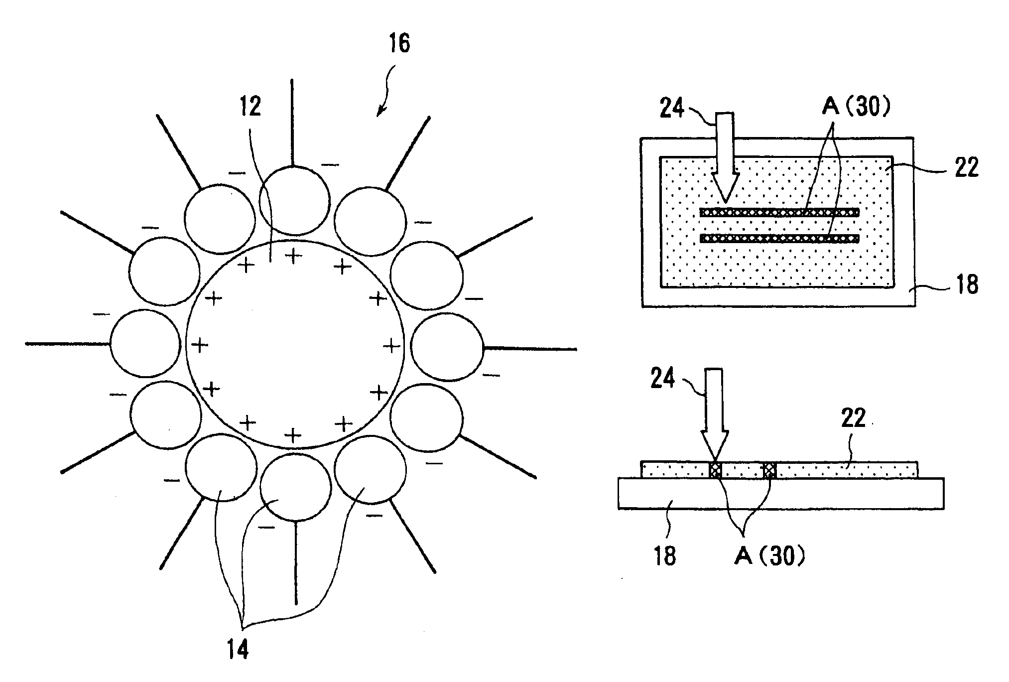
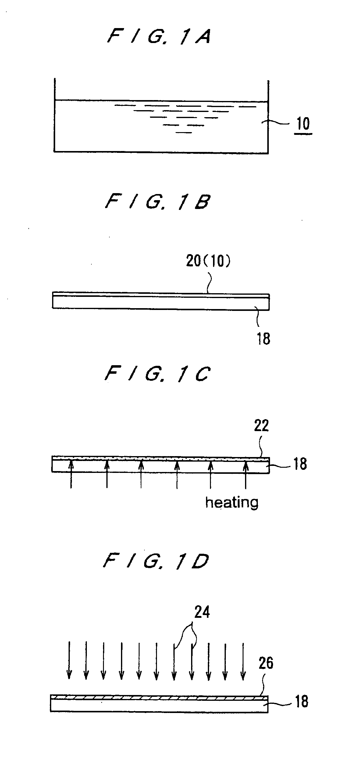
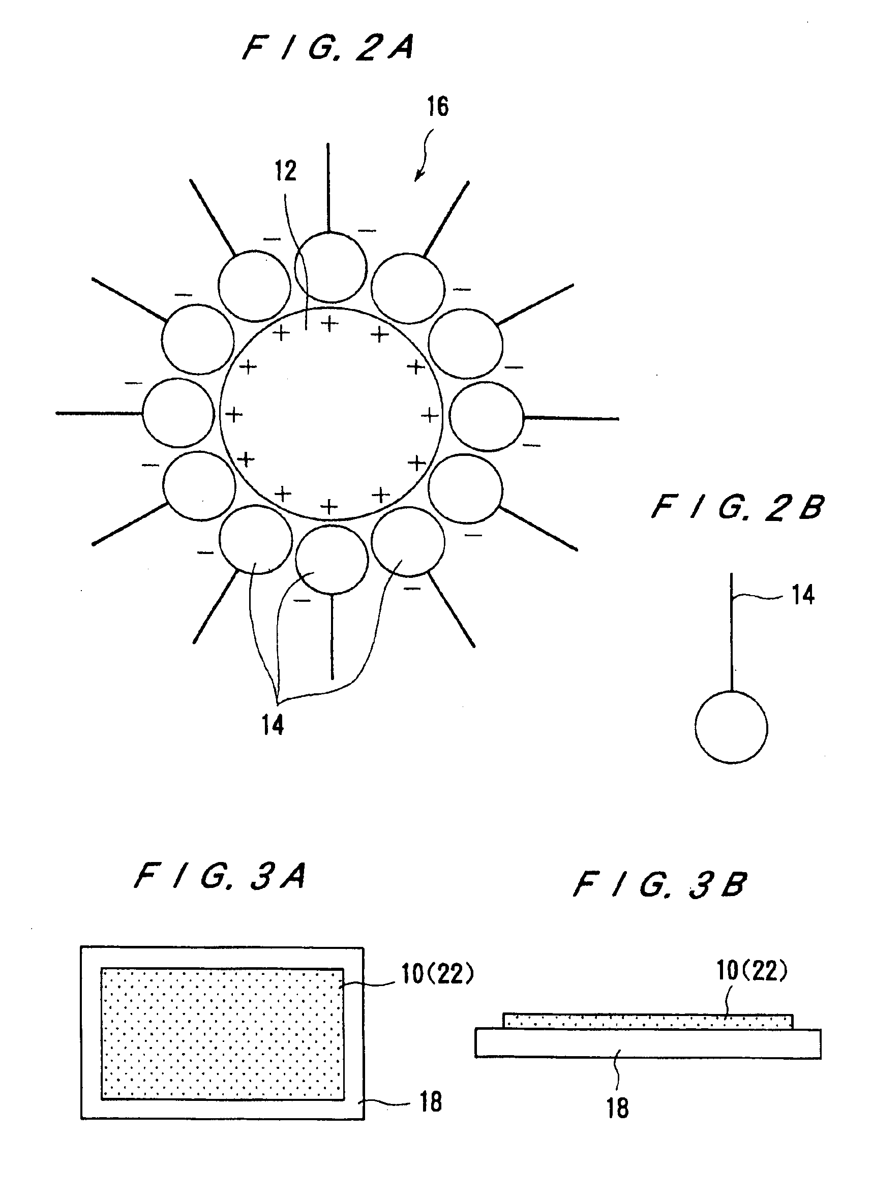
The present invention relates to a method of and an apparatus for forming a thin metal film of copper, silver, or the like on a surface of a semiconductor or another substrate. A method of forming a thin metal film, comprises preparing a dispersed liquid having a metal-containing organic compound dispersed in a predetermined solvent, coating the dispersed liquid on a surface of a substrate and evaporating the solvent to form a coating layer, and applying an energy beam to the coating layer to decompose away an organic substance contained in the coating layer in an area irradiated with the energy beam and bond metal contained in the coating layer.According to the present invention, it is possible to form a thin metal film of good quality efficiently and stably. The thin metal film used as metal interconnects in highly integrated semiconductor circuits contributes to the progress of a process of fabricating semiconductor devices.

Description

REFERENCE TO RELATED APPLICATIONS[0001]The present application is the national stage under 35 U.S.C. §371 of international application PCT / JP00 / 08418, filed Nov. 29, 2000 which designated the United States, and which application was not published in the English language.TECHNICAL FIELD[0002]The present invention relates to a method of and an apparatus for forming a thin metal film of copper, silver, or the like on a surface of a semiconductor or another substrate, and more particularly to a method of and an apparatus for forming a thin metal film to form a fine metal interconnect in a highly integrated circuit formed on a semiconductor substrate.BACKGROUND ART[0003]Aluminum or aluminum alloy has generally been used as a material for forming interconnect circuits on semiconductor substrates. It has been customary practiced to grow a film of the material according to a process such as sputtering, CVD, or the like and then form a pattern in the film according to etching or the like. As...

Claims


Application Information

Patent Timeline
Patent Type & Authority Patents(United States)
IPC IPC(8): C23C18/14H01L21/288H01L21/768H05K3/10
CPCC23C18/14H01L21/288H01L21/76885H05K3/105C23C18/143C23C18/145H01L21/3205
Inventor FUKUNAGA, AKIRAHORIE, KUNIAKIOGURE, NAOAKIKATO, TAKAONAGASAWA, HIROSHIKAJITA, SHINJIKUBOTA, MAKOTO
Owner EBARA CORP
Learn More