Method for producing high throughput strained-Si channel MOSFETS

a technology of strained silicon surface channel and mosfet, which is applied in the direction of crystal growth process, polycrystalline material growth, chemically reactive gas, etc., can solve the problems of low throughput process, complex manufacturing process, cost prohibitive, etc., and achieve low defect density and improved wafer throughput.

Inactive Publication Date: 2006-01-03
TAIWAN SEMICON MFG CO LTD
View PDF5 Cites 12 Cited by
  • Summary
  • Abstract
  • Description
  • Claims
  • Application Information

AI Technical Summary

Benefits of technology

[0008]To achieve the foregoing and other objects, and in accordance with the purposes of the present invention, as embodied and broadly described herein, the present invention provides a method for forming a strained silicon layer device with improved wafer throughput and low defect density.

Problems solved by technology

For example, most approaches for introducing strained silicon regions of the prior art employ complex multi-layer structures, for example relying on relatively thick SiGe buffer layers to achieve tensile stress in the surface silicon channel.
Conventional processes such as ultra-high-vacuum chemical vapor deposition (UHV) and molecular Beam Epitaxy (MBE) are low-throughput processes which have been economically prohibitive in applying for high throughput CMOS manufacturing processes.
In addition, although more complex devices, such as silicon-on-insulator (SOI) devices have incorporated strained silicon substrates, such devices require complex manufacturing processes which are cost prohibitive and generally incompatible with CMOS manufacturing technology.
For example, nucleation of dislocations in the strained silicon layer due to propagating strain mismatches in the SiGe layer are undesirable and attempts have been made to reduce the propagation of dislocations by various methods.
Other difficulties related to growing low defect density strained silicon layers are related to the reaction kinetics of the deposition process to epitaxially grown silicon.
However, due to several factors including the undesirable effects of thermal gradients which contribute to dislocation nucleation, lower temperature epitaxial growth is frequently a preferred process.

Method used


Image

  • Method for producing high throughput strained-Si channel MOSFETS
  • Method for producing high throughput strained-Si channel MOSFETS
  • Method for producing high throughput strained-Si channel MOSFETS

Examples


Embodiment Construction

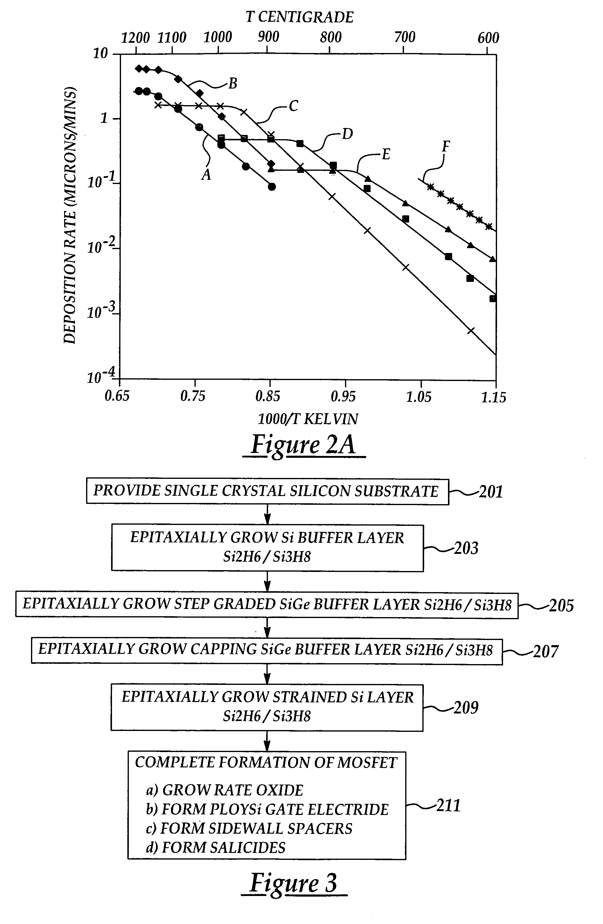
[0014]Although the method of the present invention is explained with reference to a particular strained-Si channel N-MOFSET device, it will be appreciated that the method of the present invention may be applied to the formation of P-MOFSET devices as well. In addition, although an exemplary strained-Si channel multi-layered device is presented as an exemplary implementation and embodiment of the invention it will be appreciated that the method of the present invention may be advantageously used to increase a deposition rate and thereby decrease a process cycle time to increase a wafer throughput in the formation of any strained-Si layer device.

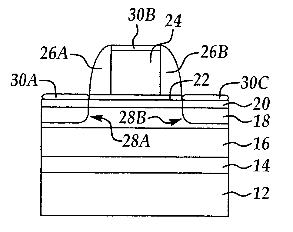
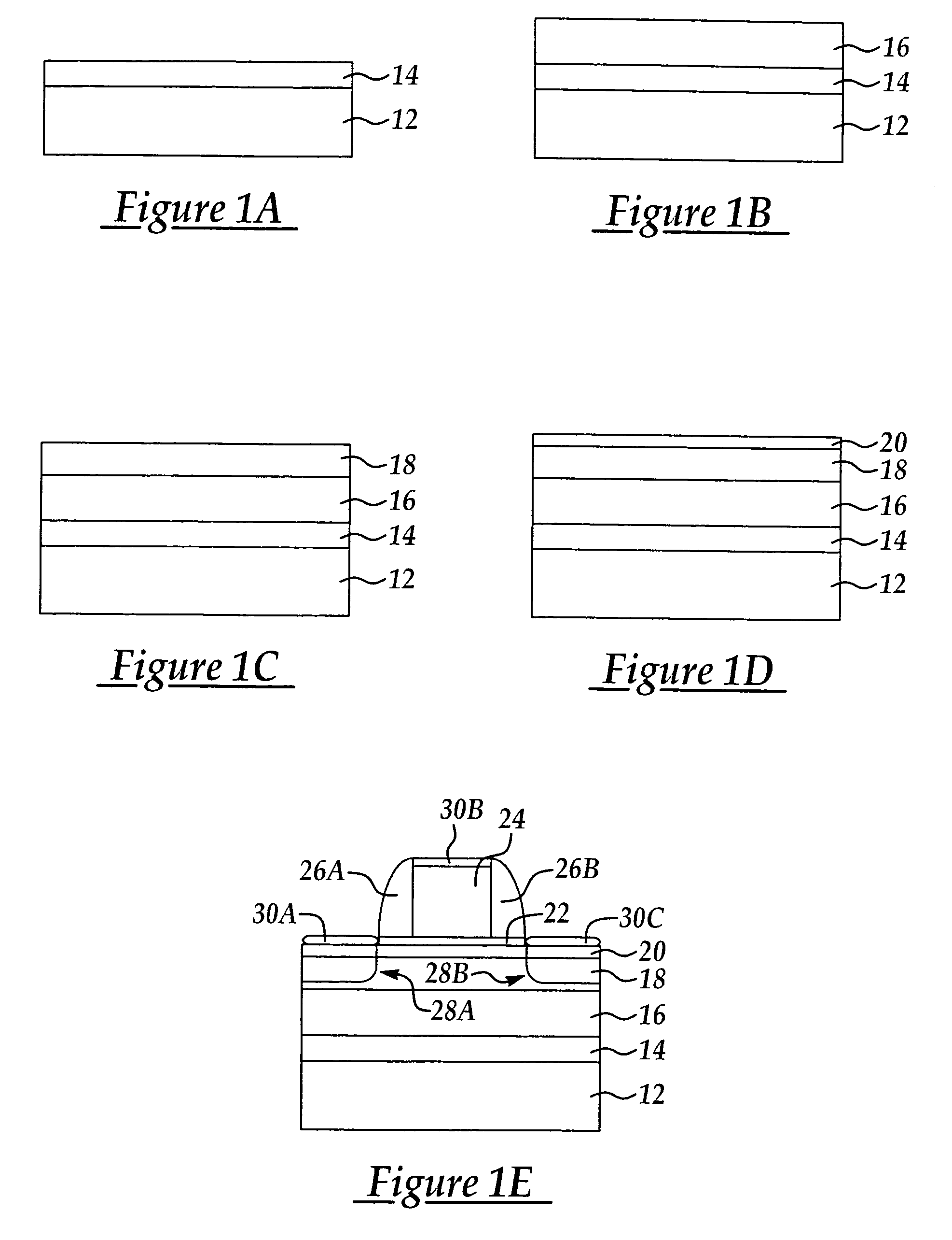
[0015]Referring to FIGS. 1A–1E, in an exemplary embodiment of the method of the present invention are shown cross-sectional schematic views of a portion of a semiconductor wafer at stages in production of an exemplary strained-Si channel N-MOFSET device.

[0016]Referring to FIG. 1A, a substrate (silicon wafer) 12 formed of single crystalline sil...


PUM

PropertyMeasurementUnit
temperatureaaaaaaaaaa

Abstract

A method for forming a strained silicon layer device with improved wafer throughput and low defect density including providing a silicon substrate; epitaxially growing a first silicon layer using at least one deposition precursor selected from the group consisting of disilane and trisilane; epitaxially growing a step-grade SiGe buffer layer over and contacting the first silicon layer using at least one deposition precursor selected from the group consisting of disilane and trisilane; epitaxially growing a SiGe capping layer over and contacting the step-grade SiGe buffer layer using at least one deposition precursor selected from the group consisting of disilane and trisilane; and, epitaxially growing a second silicon layer using at least one deposition precursor selected from the group consisting of disilane and silane.

Description

FIELD OF THE INVENTION[0001]This invention generally relates to micro-integrated circuit manufacturing and more particularly, to epitaxial growth methods for producing strained silicon surface channel MOSFET devices.BACKGROUND OF THE INVENTION[0002]An increasingly sought after approach for improving the performance of a metal oxide semiconductor field effect transistor (MOSFET), including a complimentary metal oxide semiconductor (CMOS) device is the introduction of strain induced band modification. Several approaches have been made to produce Strained Si-channel N and P MOSFETS with varying degrees of success.[0003]One approach to producing a strained silicon channel, for example one in tensile strain, is by growing a thin silicon channel layer over step-graded SiGe. One implementation of a tensile strained Si channel is the growth of silicon over a relatively thick SiGe substrate. For example, most approaches for introducing strained silicon regions of the prior art employ complex...

Claims


Application Information

Patent Timeline
Patent Type & Authority Patents(United States)
IPC IPC(8): H01L21/30C30B1/00C30B25/02H01L21/20H01L21/205H01L21/306H01L21/36H01L21/44
CPCC30B25/02H01L21/02381H01L21/0245H01L21/02505H01L29/7842H01L21/02532H01L21/0262C30B29/52H01L21/02052
Inventor LEE, KUEN-CHYRYAO, LIANG-GICHEN, SHIH-CHANGLIANG, MONG-SONG
Owner TAIWAN SEMICON MFG CO LTD
Why Eureka
Try Eureka