Light emitting device

a technology of light emitting device and light source, which is applied in the direction of discharge tube luminescnet screen, discharge tube/lamp details, electric discharge lamps, etc., can solve the problems of difficult in many directions, hindering cost reduction, and affecting the stability of the driver of the element, so as to improve the driver stability of the element and reduce the cost. , the effect of low cos

Inactive Publication Date: 2006-01-31
SEMICON ENERGY LAB CO LTD
View PDF26 Cites 9 Cited by
  • Summary
  • Abstract
  • Description
  • Claims
  • Application Information

AI Technical Summary

Benefits of technology

[0030]Thus, since local concentration of an electric field can be prevented, it is considered that dielectric breakdown, deterioration of a material, and the like are suppressed. Therefore, there is a possibility that an element structure disclosed by the present invention leads a long life of an element. It is said that an effect in which an improvement of driver stability of the element may be expected is one of important characteristics of the present invention.
[0031]From the above reason, when the present invention is embodied, it is possible to provide an organic EL element in which light emission efficiency is high, can be manufactured using a conventional organic compound with low costs, and can be operated as stable as possible.

Problems solved by technology

Also, all generated lights are not emitted to the outside and a portion of the lights cannot be picked up because of the refractive indexes inherent to organic EL element constituent substances (organic compound layer and electrodes) and a substrate.
However, since both platinum and iridium are so-called noble metal, the platinum complex and the iridium complex using these metals are expensive and thus it is expected that a cost reduction is hindered in future.
However, a clear molecular design plan is not established until now and it is very difficult in many sides.
Also, with respect to the organic EL elements capable of converting the triplet excitation energy into light to be emitted, as described in References 2 and 3, there is a problem in an element life, that is, the half life of intensity does not reach a practicable level.

Method used


Image

  • Light emitting device
  • Light emitting device
  • Light emitting device

Examples


embodiment 1

[Embodiment 1]

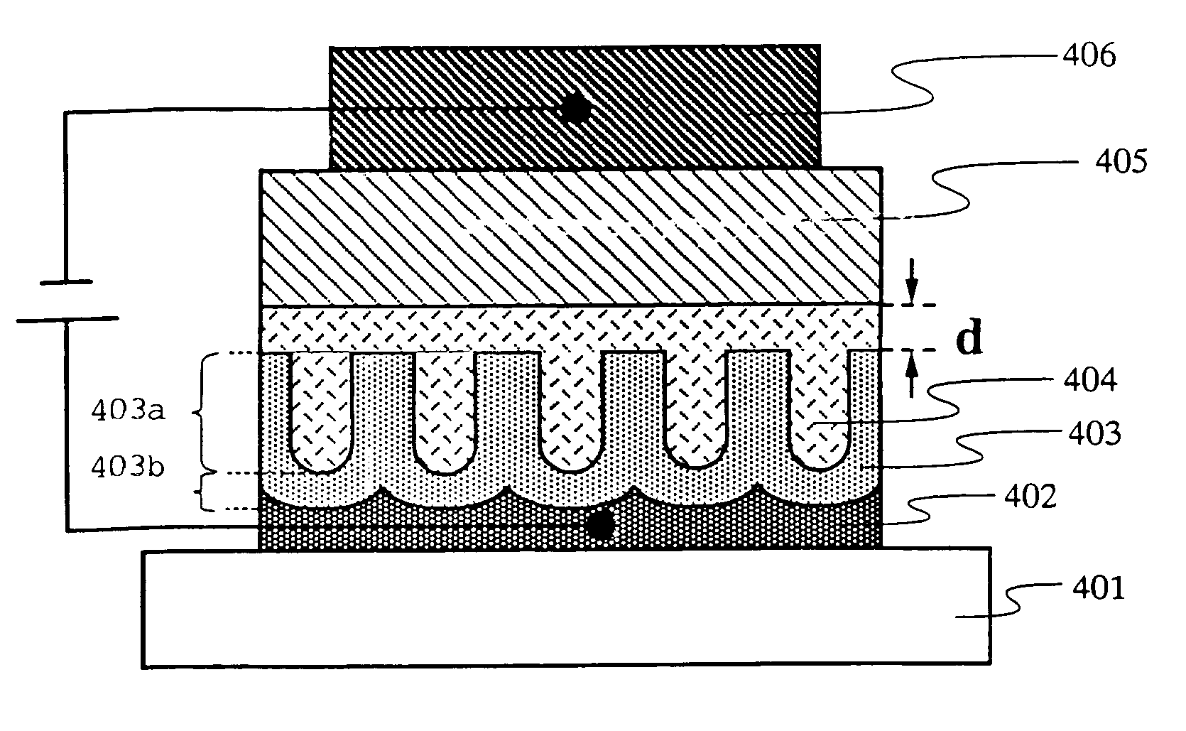
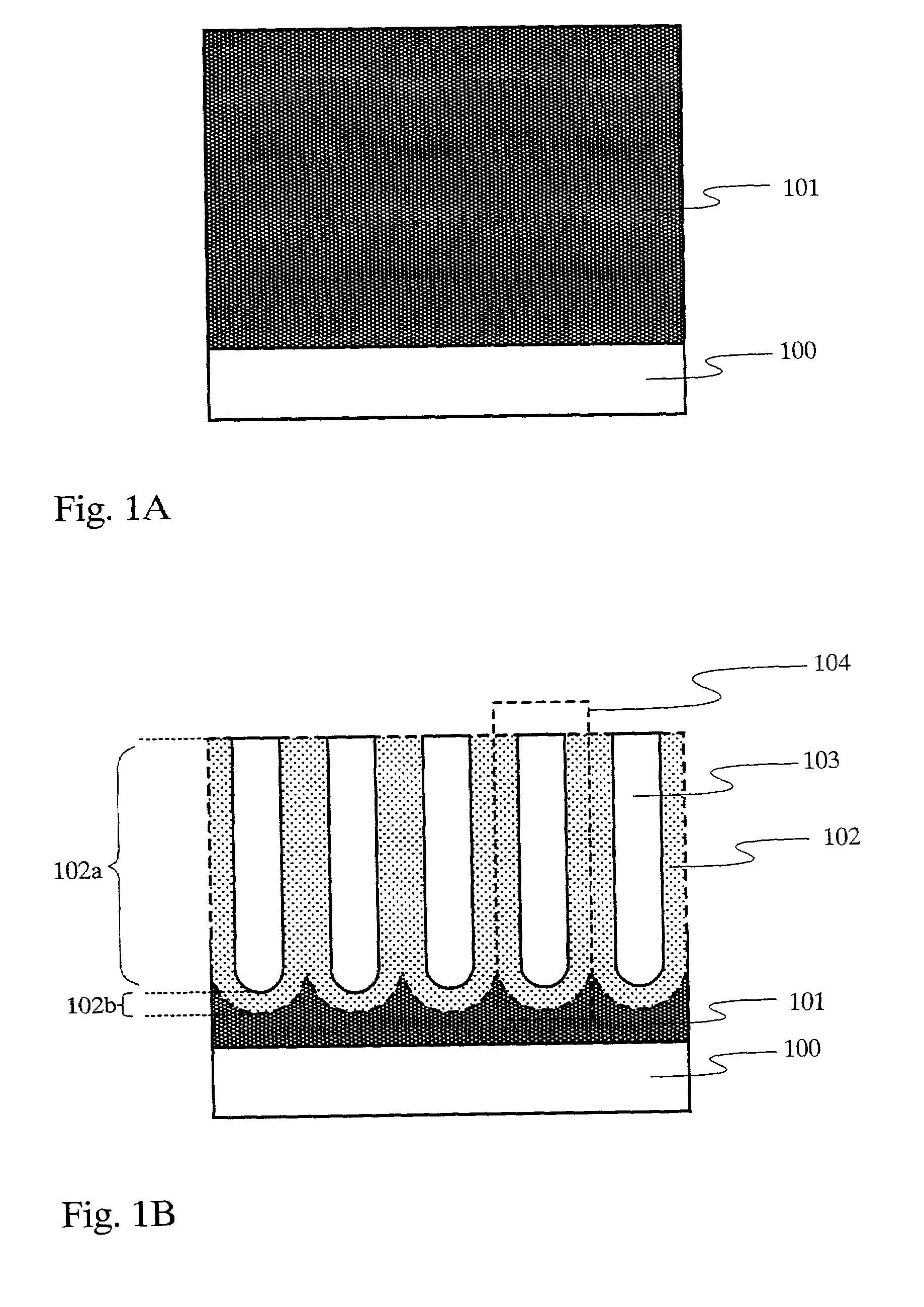
[0077]In this embodiment, an element in which a porous oxide film is formed using anodization, as shown in FIGS. 1A and 1B will be described with a concrete example. A method in which a pixel electrode is formed using tantalum (Ta), an anodization is performed using Ta as the anode, and a film is formed from the anode side will be described with an example. An element structure is shown in FIG. 4.

[0078]First, Ta is formed as an anode layer 402 on a glass substrate 401 by sputtering. At this point, it is required that a Ta film to be formed has a sufficient thickness (˜1 μm). This is because the film surface becomes an oxide film by anodization processing as described later.

[0079]Next, anodization processing is performed using the formed Ta film as an anode in an oxalic acid solution to form an oxide film 403. The oxide film 403 is composed of a porous layer 403a having pores vertical to the film surface and a barrier layer 403b in which the number of holes is relativel...

embodiment 2

[Embodiment 2]

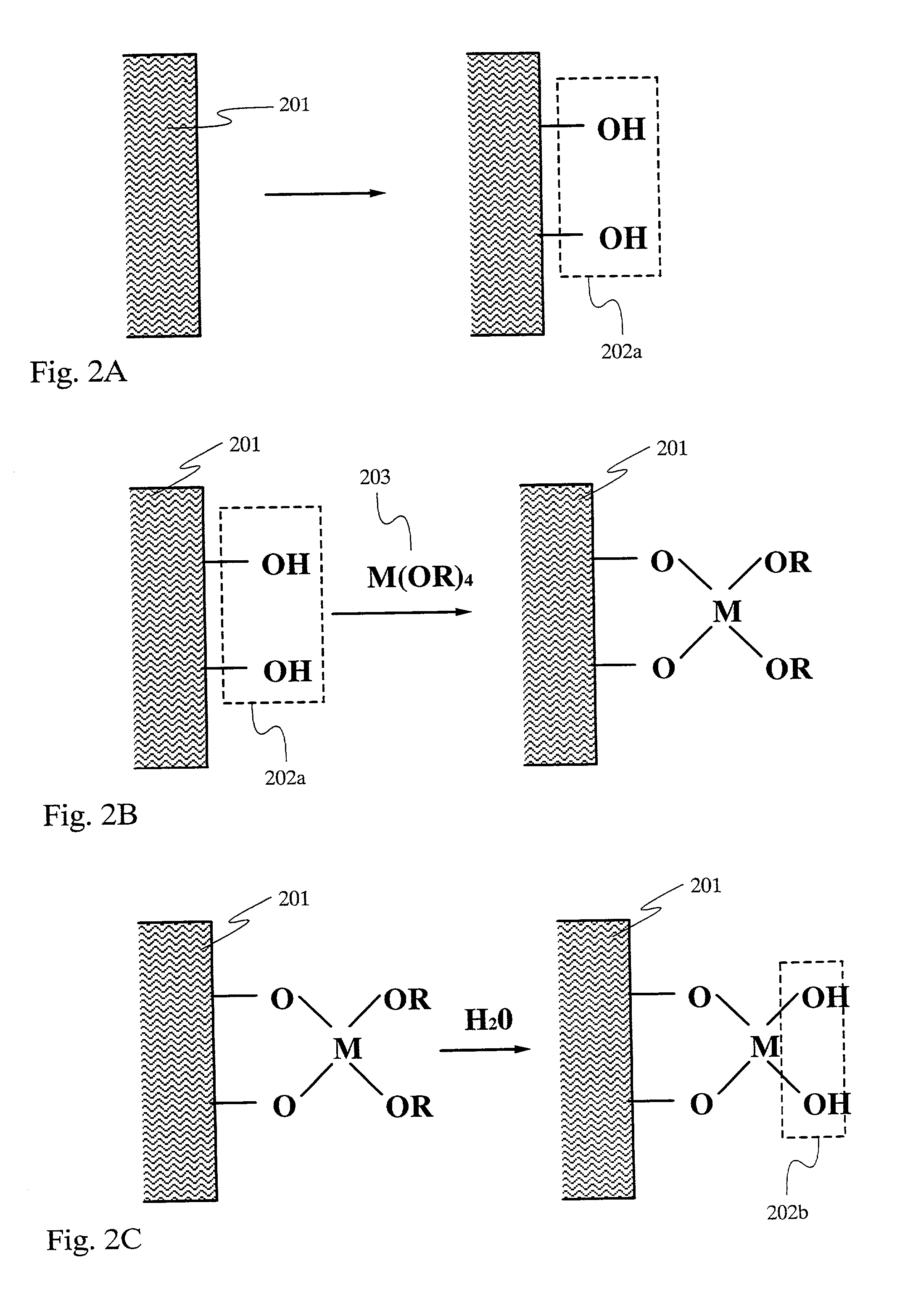
[0085]In this embodiment, an element in which a metal oxide porous body is formed using a sol-gel method, as shown in FIGS. 2A to 2C will be described with a concrete example. In a case of sol-gel method, the pixel electrode is formed using Ta or indium tin oxide (ITO) since the metal oxide porous is formed besides the electrode. A method of forming a film from an anode layer side using tantalum (Ta) as the anode layer will be described with an example. An element structure is shown in FIG. 5.

[0086]First, Ta is formed as an anode layer 502 on a glass substrate 501 by sputtering. A Ta film formed in this embodiment preferably has a thickness such as it sufficiently functions as an electrode (concretely, about 100 nm).

[0087]Next, an oxide porous layer 503 (Ta2O5 in this embodiment) is formed on the anode layer 502 by a surface sol-gel method. Penta-n-propoxytantalum (Ta(O-n-C3H7)5; liquid in a room temperature)) is used as a raw. First, the anode layer 502 for which hydr...

embodiment 3

[Embodiment 3]

[0094]In this embodiment, an element into which zeolite is introduced as a metal oxide porous body, as shown in FIGS. 3A and 3B will be described with a concrete example. In case of introducing zeolite, the metal oxide porous body is formed besides the electrode. An organic EL element manufacturing method of forming a film from the side of a transparent electrode (an anode layer), which is a pixel electrode, will be described with an example. An element structure is shown in FIG. 6.

[0095]First, the indium tin oxide (ITO) which is a transparent electrode is formed as an anode layer 602 on a glass substrate 601 by sputtering and then coated with an aqueous solution of sodium silicate and sodium aluminate. Then, thermal treatment is performed at 100° C. for 6 hours to form zeolite X (cation metal is sodium) (a zeolite film 603).

[0096]Next, when the promotion of phosphorescence by the heavy atom effect is considered, the cation metal of the zeolite X is transformed from so...


PUM


Abstract

There is provided a light emitting device and electric equipment, which are bright and have low consumption power and are low in costs. When an organic EL material is made present in a metal oxide porous body including a heavy atom, phosphorescence light emitting of the organic EL material in which only fluorescence is generally observed can be promoted. Thus, an organic EL element in which phosphorescence light emitting is produced is obtained. With respect to this element, since phosphorescence can be used, light emitting efficiency is high. Also, since a conventional organic EL material can be used, it can be manufactured with a low cost. A light emitting device and electric equipment are manufactured using this organic EL element.

Description

BACKGROUND OF THE INVENTION[0001]1. Field of the Invention[0002]The present invention relates to a light emitting device using as a light source an element (hereinafter referred to as “an organic EL element”) which is composed of an anode layer, a cathode layer, and a layer including an organic compound (hereinafter referred to as “an organic compound layer”) in which an electroluminescence (hereinafter referred to as “an EL”) is generated by applying an electric field thereto. The EL in the organic compound includes luminescence generated when it is returned from a singlet excitation state to a ground state (fluorescence) and luminescence generated when it is returned from a triplet excitation state to a ground state (phosphorescence). In particular, the present invention relates to a light emitting device in which a porous body of an inorganic material is made in contact with an organic compound layer and thus the generation of phosphorescence is promoted. Note that a light emitti...

Claims


Application Information

Patent Timeline
Patent Type & Authority Patents(United States)
IPC IPC(8): H05B33/26H05B33/00H05B33/14H01L51/50H01L51/52
CPCH01L51/5012H01L51/5221H01L51/5206H01L51/5048H10K50/155H10K50/165H10K50/14H10K50/81H10K50/11H10K2101/10H10K50/82H05B33/14
Inventor SEO, SATOSHI
Owner SEMICON ENERGY LAB CO LTD
Why Eureka
Try Eureka