Direct-write laser transfer and processing

a laser transfer and laser technology, applied in the field of material deposition, can solve the problems of inability to adapt to large-scale rapid prototyping, limit the flexibility and capability of these approaches, and wet techniques are inherently limited by viscoelastic properties

Inactive Publication Date: 2006-03-21
NAVY UNITED STATES OF AMERICA AS
View PDF23 Cites 58 Cited by
  • Summary
  • Abstract
  • Description
  • Claims
  • Application Information

AI Technical Summary

Benefits of technology

[0017]It is an object of the present invention to provide a device and method that allows for laser transfer and laser processing of a material to occur in sequential steps.

Problems solved by technology

(Direct writing may also be accomplished in the sub-micron range using electron beams or focused ion beams, but these techniques, because of their small scale, are not appropriate for large scale rapid prototyping.)
The solvent or binder must later be removed by a drying or curing process, which limits the flexibility and capability of these approaches.
In addition, wet techniques are inherently limited by viscoelastic properties of the fluid in which the particles are suspended or dissolved.
Because the film material is vaporized by the action of the laser, laser induced forward transfer is inherently a homogeneous, pyrolytic technique and typically cannot be used to deposit complex crystalline, multi-component materials or materials that have a crystallization temperature well above room temperature because the resulting deposited material will be a weakly adherent amorphous coating.
Moreover, because the material to be transferred is vaporized, it becomes more reactive and can more easily become degraded, oxidized or contaminated.
The method is not well suited for the transfer of organic materials, since many organic materials are fragile and thermally labile and can be irreversibly damaged during deposition.
Moreover, functional groups on an organic polymer can be irreversibly damaged by direct exposure to laser energy.
Other disadvantages of the laser induced forward transfer technique include poor uniformity, morphology, adhesion, and resolution.
Further, because of the high temperatures involved in the process, there is a danger of ablation or sputtering of the support, which can cause the incorporation of impurities in the material that is deposited on the receiving substrate.
Another disadvantage of laser induced forward transfer is that it typically requires that the coating of the material to be transferred be a thin coating, generally less that 1 μm thick.
Because of this requirement, it is very time-consuming to transfer more than very small amounts of material.
A disadvantage of this method is that, because of the multiple layers, it is difficult or impossible to achieve the high degree of homogeneity of deposited material on the receiving substrate required, for example, for the construction of electronic devices, sensing devices or passivation coatings.
A limitation of both processes is that they must be carried out under controlled atmospheres such as inside a vacuum system and they tend to exhibit slow deposition rates.
In addition, they are not well suited for direct write applications where multilayers of dissimilar materials need to be produced.
LENS is a process that works well for making thick layers of metals, however, the high melting points exhibited by most ceramics required the use of high power laser beams that cause overheating of the substrate and surrounding layers.
Furthermore, many ceramics once melted will not exhibit their original crystalline structure after solidification.
In addition, because the materials being deposited must first melt and then resolidify, the layers are under large stresses which can cause their delamination.
There are some materials that are easier to transfer in a precursor state or as a mixture of a precursor and a powdered form, but when they are transferred in this form, they do not have desired physical properties such as electrical conductance.

Method used


Image

  • Direct-write laser transfer and processing
  • Direct-write laser transfer and processing

Examples


example 2

Laser Transfer and Processing of Barium Titanate (BaTiO3)

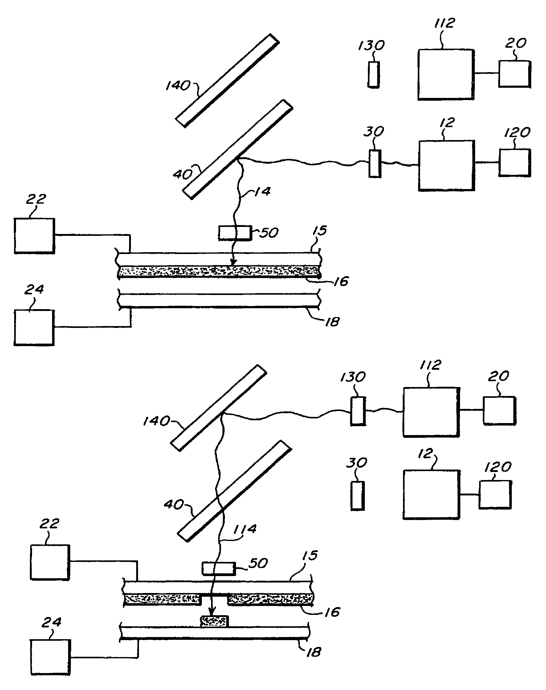
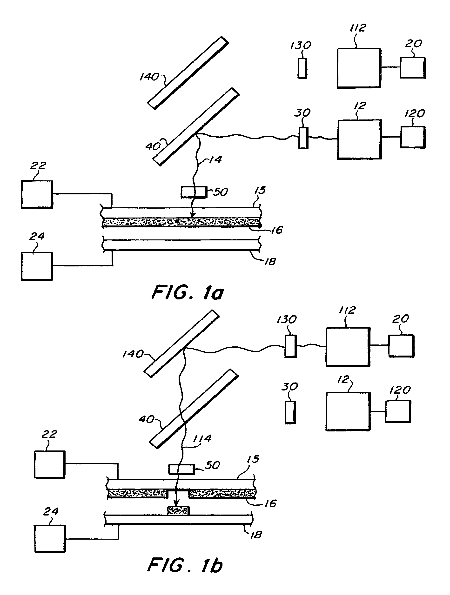
[0055]Using a method similar to that described in example 1), the ferroelectric material BaTiO3 (BTO) was transferred to interdigitated capacitor structures on an MgO substrate.

[0056]The receiving substrate has interdigitated capacitors of various finger lengths and gap spacings patterned on a (500 Å)Au / (1.5 μm)Ag / (500 Å)Cr coating on an MgO substrate. The target substrate consisted of a mixture of BTO powders in a precursor agent comprising barium neodecanoate and dimethoxy titanium dineodecanaoate deposited as a layer on one side of a UV-grade fused silica disk.

[0057]The UV transfer laser wavelength was 248 nm and the focal laser fluence on the target substrate was 0.3 J / cm2. The focal spot size was 40 microns in diameter. The UV laser operated at 1 Hz and the target substrate was moved after every laser shot to expose a fresh area of the BTO coating. (A 25-micron spacer was used between the target and receiving substrates)....


PUM

PropertyMeasurementUnit
temperatureaaaaaaaaaa
thickaaaaaaaaaa

Abstract

A device and method for depositing a material of interest onto a receiving substrate includes a first laser and a second laser, a receiving substrate, and a target substrate. The target substrate comprises a laser transparent support having a back surface and a front surface. The front surface has a coating that comprises the source material, which is a material that can be transformed into the material of interest. The first laser can be positioned in relation to the target substrate so that a laser beam is directed through the back surface of the target substrate and through the laser-transparent support to strike the coating at a defined location with sufficient energy to remove and lift the source material from the surface of the support. The receiving substrate can be positioned in a spaced relation to the target substrate so that the source material is deposited at a defined location on the receiving substrate. The second laser is then positioned to strike the deposited source material to transform the source material into the material of interest.

Description

[0001]This application claims the benefit of U.S. Provisional Application No. 60 / 144,662, filed Jul. 19, 1999.BACKGROUND OF THE INVENTION[0002]1. Field of the Invention[0003]The invention relates generally to the deposition of materials and more specifically, to devices, materials and methods for direct writing of a source material onto a substrate using a first laser and then transforming the source material into a material of interest by means of a second laser.[0004]2. Description of the Related Art[0005]The term “direct write” refers generally to any technique for creating a pattern directly on a substrate, either by adding or removing material from the substrate, without the use of a mask or preexisting form. Direct write technologies have been developed in response to a need in the electronics industry for a means to rapidly prototype passive circuit elements on various substrates, especially in the mesoscopic regime, that is, electronic devices that straddle the size range be...

Claims


Application Information

Patent Timeline
Patent Type & Authority Patents(United States)
IPC IPC(8): C23C14/28B05D3/00C23C14/30
CPCC23C14/048C23C14/088C23C14/14C23C14/28C23C14/5813H05K3/046H05K2203/121H05K3/105H05K2203/0528H05K2203/107H05K2203/108
Inventor PIQUE, ALBERTOAUYEUNG, RAYMONDFITZGERALD, JAMESCHRISEY, DOUGLAS B.WU, HUEY-DAWKYDD, PAULRICHARD, DAVID L.
Owner NAVY UNITED STATES OF AMERICA AS
Why Eureka
Try Eureka