

Two-dimensionally arrayed quantum device
a quantum device and two-dimensional array technology, applied in nanoinformatics, instruments, coatings, etc., can solve the problems of unstable single-electron memory based on polycrystal si film, unstable single-electron transistor operation at 100 k, and far below room temperature. , to achieve the effect of not being practical use, and being unstabl
- Summary
- Abstract
- Description
- Claims
- Application Information
AI Technical Summary
Benefits of technology
Problems solved by technology
Method used
Image

Examples
embodiment 1
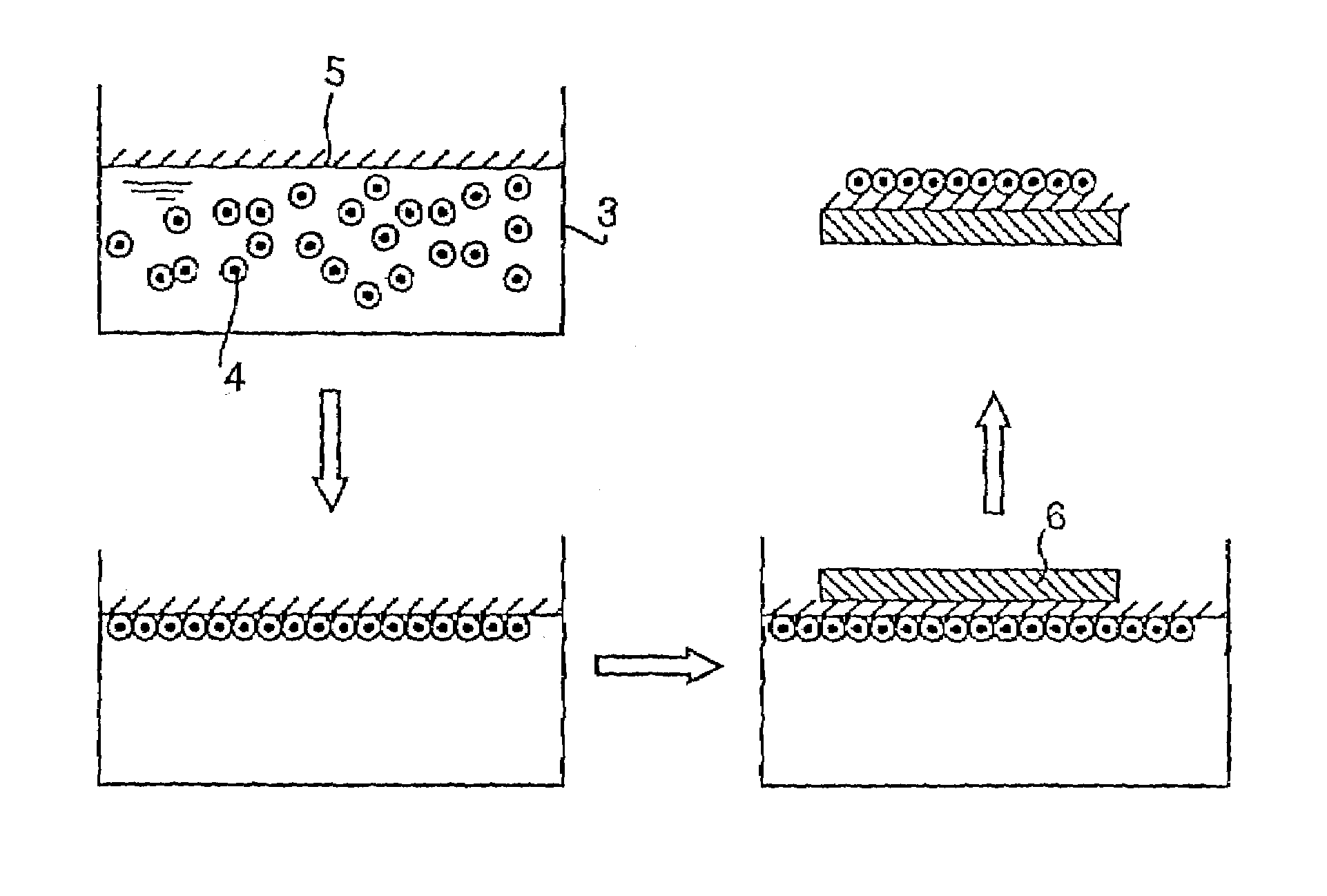
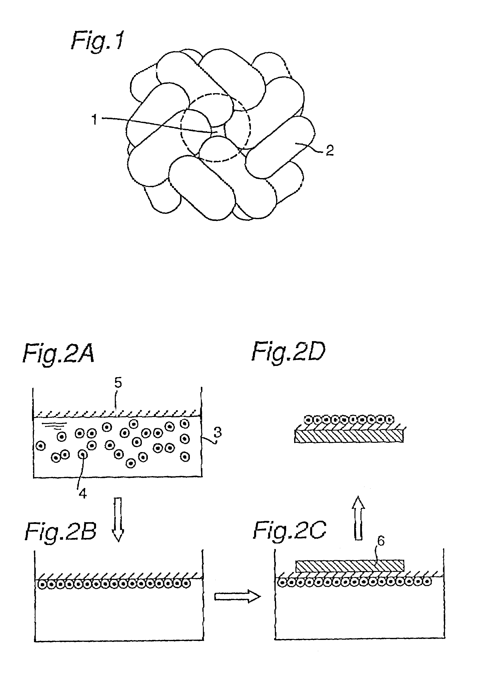
[0054]The first embodiment of the present invention is an example of a method for manufacturing a quantum device. A solution of ferritin is prepared. Ferritin is a metalloprotein complex comprising a core 1 of Fe2O3 enclosed in a shell 2 of a protein as shown in FIG. 1, which can be extracted from organs such as a spleen or liver of animals such as a horse or cow. The core 1 has a diameter of about 6 nm, and includes from 1000 to 3000 iron atoms. The shell 2 is a trisoctamer of protein having a molecular weight of about 20,000. The trisoctamer measures about 12 nm across.
[0055]As shown in FIG. 2A, a tank 3 made of teflon is filled with a buffer liquid wherein ferritin 4 is dispersed and PBLH membrane (polypeptide membrane) 5 is spread on the liquid surface. Hydrogen ion concentration of the liquid is controlled to about pH6 by using a proper acid, for example, hydrochloric acid. Because the PBLH membrane 5 is positively charged and the ferritin 4 is negatively charged, ferritin 4 is...
embodiment 2
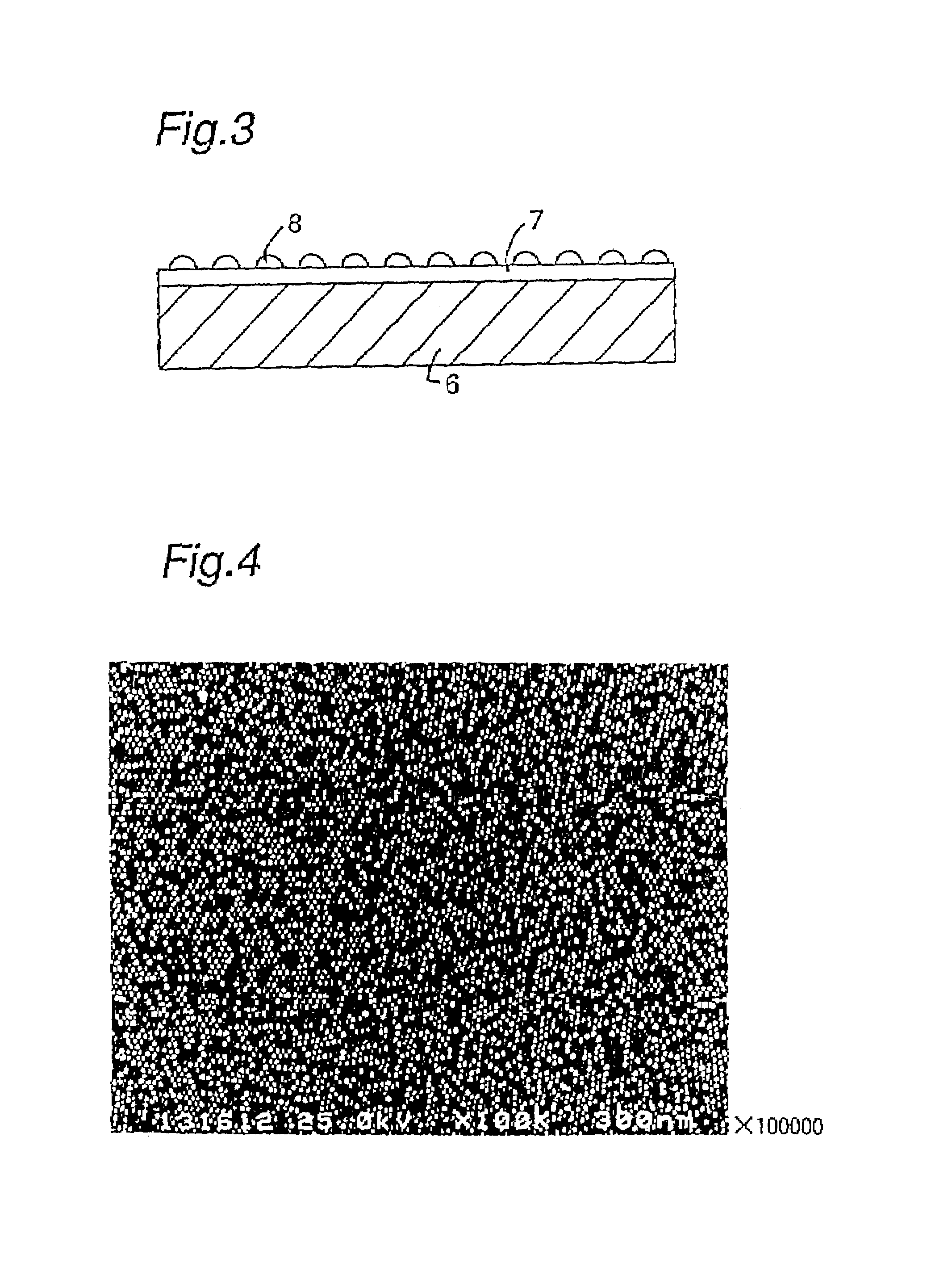
[0058]This embodiment is an example of wiring method for the quantum device obtained in the first embodiment. The quantum device obtained in the first embodiment is put in the chamber of a field emission scanning electron microscope (FE-SEM), the inside of the chamber being a pumped vacuum to about 10−6 Pa. An electron beam with a width being set to about 5 nm is scanned between the drain D, the source S or the gate G and one or more of the iron atom aggregates M1 through M3. This results in a lead wire made of carbon 20 nm wide connecting the drain, the source, the gate and the iron atom aggregates M1 through M3 and electrodes M1 through M3 being formed.
embodiment 3
[0059]The third embodiment is an example of the diode of the present invention. A column filled with polystyrene beads of mean diameter 100 μm having ammonium radical NH4+ bonded onto the surface thereof is prepared. Aluminum oxide is put in a position of an apoferritin core, and metal-apoferritin complex thus obtained is passed through the column to be absorbed onto the polystyrene beads. Then, phosphoric acid is put in a position of another apoferritin core, and metal-apoferritin complex thus obtained is passed through the same column to be absorbed onto the polystyrene beads. The two kinds of metal-apoferritin complex are made to bond by a disulfide linkage between sulfur atoms of a cysteine residue of protein, thereby fabricating a hetero-dimer shown in FIG. 6. The hetero-dimer is let to flow out of the column into the same tank as that of the first embodiment.
[0060]Under the same conditions as those of the first embodiment, except that the ferritin of the first embodiment is re...
PUM
| Property | Measurement | Unit |
|---|---|---|
| thickness | aaaaa | aaaaa |
| thickness | aaaaa | aaaaa |
| thickness | aaaaa | aaaaa |
Abstract
Description
Claims
Application Information