Ultra-thin Si channel CMOS with improved series resistance

a series resistance, ultra-thin technology, applied in the direction of basic electric elements, electrical equipment, semiconductor devices, etc., can solve the problems of increasing the possible clock rate, reducing the propagation time and susceptibility of signals, and the length of signal propagation paths, so as to achieve improved series resistance and low thermal budget processing

Active Publication Date: 2006-03-28
TWITTER INC
View PDF25 Cites 26 Cited by
  • Summary
  • Abstract
  • Description
  • Claims
  • Application Information

AI Technical Summary

Benefits of technology

[0010]It is therefore an object of the present invention to provide a method for simultaneously achieving CMOS devices on ultra-thin Si channels having improved series resistance, extensions undergoing low thermal budget processing and independent pFET and nFET offset.
[0011]It is another object of the invention to provide a method and structure to produce a high performance pFET and nFET device on the same wafer.
[0012]It is another object of the invention to allow the silicide to be significantly closer to the channel region thereby increasing the electron mobility and providing lower external resistance.
[0013]In order to accomplish these and other objects of the invention, a method of improving the performance of different semiconductor conductivities on the same wafer will be provided comprising steps of fabricating thin spacers on a wafer, forming raised source-drain regions by selective epitaxy, depositing a hard mask film across the wafer, forming a block mask over a first transistor, removing the block film stack from a second transistor, removing said block mask over the first transistor, performing additional selective epitaxial growth affecting only the areas of the second transistor as the block film stack covering the first transistor is resistant to the additional epitaxial procedure, and performing extension implants to the first and / or second transistor.

Problems solved by technology

That is, increased integration density and proximity of elements reduces the signal propagation path length and reduces signal propagation time and susceptibility to noise and increases possible clock rates while the reduction in element size necessary for increased integration density increases the ratio of functionality which can be provided on a chip to the costs of production (e.g. wafer / chip area and process materials) per chip and, potentially, the cost of devices containing the chips by reducing the number of inter-chip and inter-board connections required.
Although these attributes are highly desirable, thin silicon channel Si devices have significant disadvantages that could hinder further SOI CMOS scaling.
The primary disadvantage is that as the SOI film is thinned, the series resistance increases.
This causes at least two problems.
The first problem is that since the pFET extension requires a fairly thick offset spacer, a high resistance region exists under the spacer.
The second problem is that since the extension implants are performed prior to the RSD process, the dopants are subjected to the significant thermal budget of the RSD process.
This can cause unwanted diffusion of the dopants.
Also, the surface concentration of the dopants must be uniform across the wafer as well as from wafer to wafer, which is a major challenge, if the RSD process is to be manufacturable.
Although the disposable spacer scheme overcomes the problem of subjecting the extensions to the RSD thermal budget, this process does not overcome the problem of the high-resistance region outside the RSD layer.
However, the arsenic source and drain regions 128 of the nFET 100 do not adequately diffuse yielding poor performance and a high level of resistance under the thick spacer.
Such a configuration, however, has not been practical due to the increase of process steps to form spacers of different thicknesses.

Method used


Image

  • Ultra-thin Si channel CMOS with improved series resistance
  • Ultra-thin Si channel CMOS with improved series resistance
  • Ultra-thin Si channel CMOS with improved series resistance

Examples


Embodiment Construction

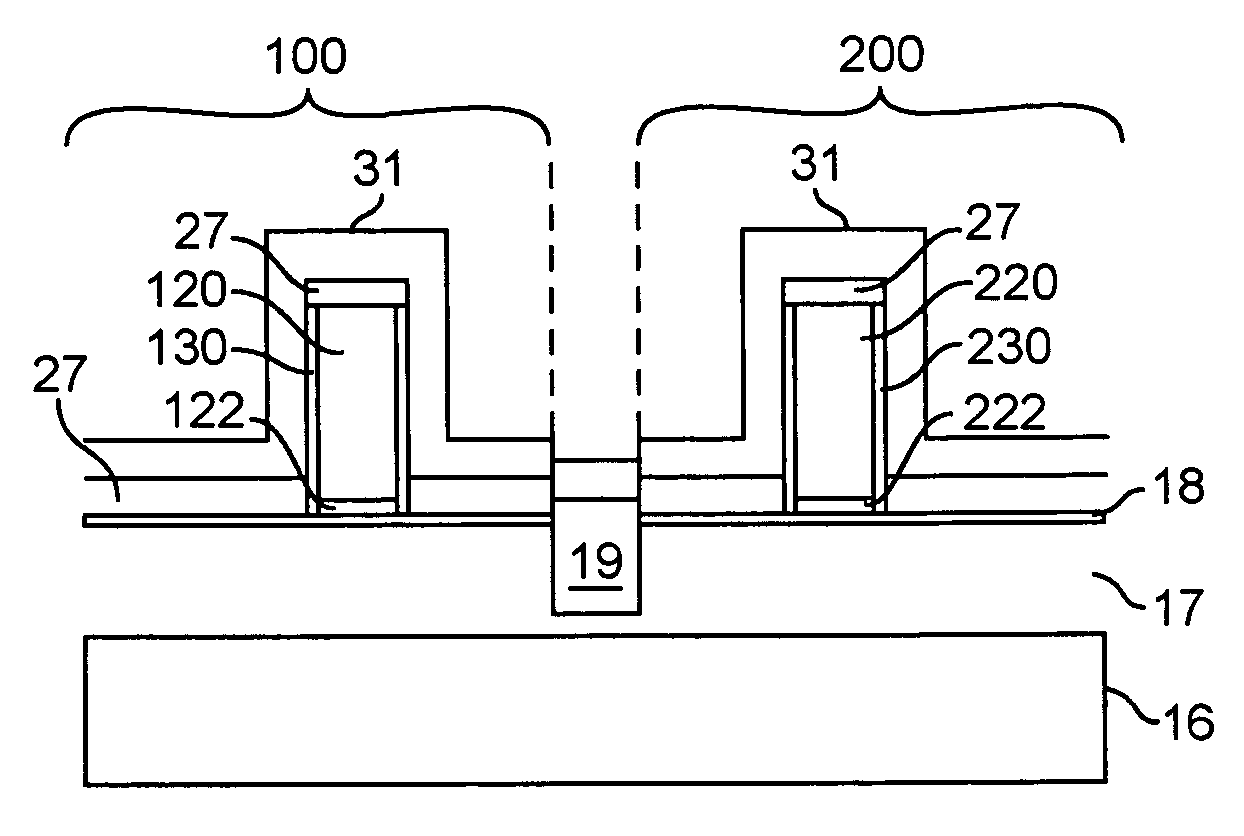
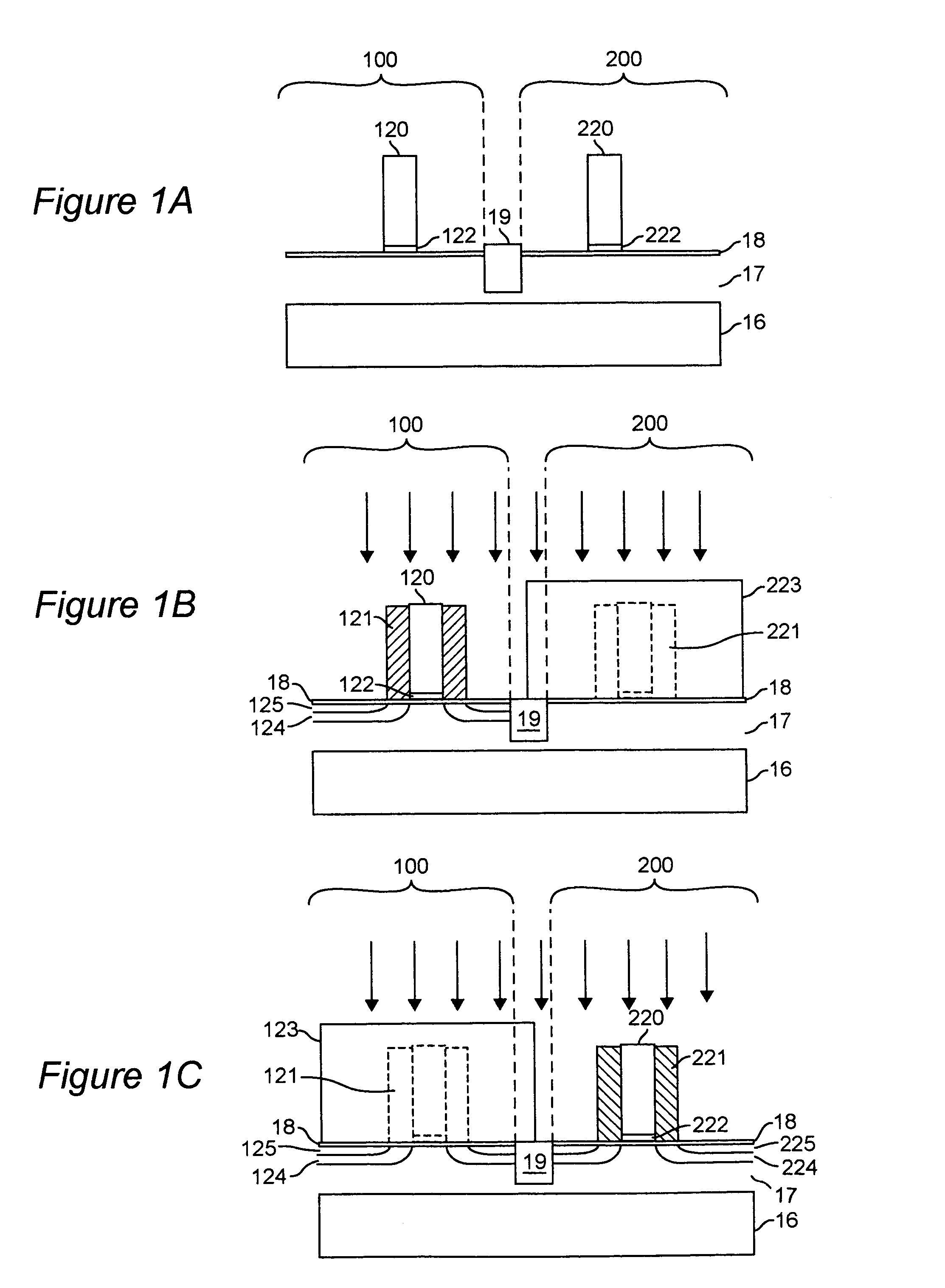
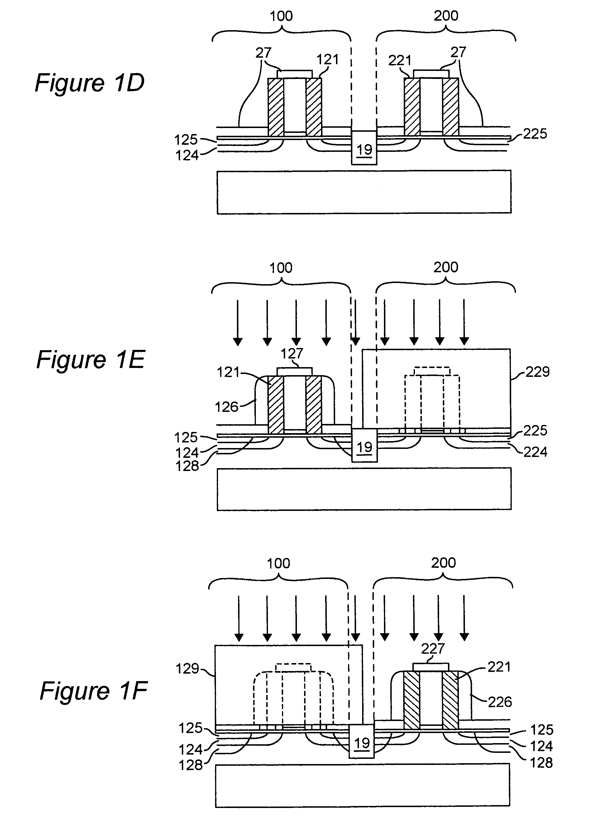
[0033]Referring now to the drawings, and more particularly to FIGS. 1a–1f, a method over which the invention provides improvements is shown for forming a CMOS pair. FIGS. 1a–1f are arranged to provide an enhanced understanding of the invention and no portion thereof is admitted to be prior art as to the present invention. The process shown in these steps exhibits particular deficiencies which the present invention successfully avoids. More specifically, FIG. 1a is a cross-sectional view of an SOI device including an Si substrate 16, isolation layer 17, oxide layer 18, gate dielectrics 122, 222, and a patterned gate stacks 120, 220. FIG. 1b illustrates the next step in this process, where spacers 121 are formed in the nFET region 100 and spacers 221 are formed over the pFET region 200. The pFET region 200 is protected using a block out mask 223 while the nFET region 100 has extensions 125 and halos 124 implanted. The mask 223 is removed from the pFET region 200 and another block mask...


PUM


Abstract

Thin silicon channel SOI devices provide the advantage of sharper sub-threshold slope, high mobility, and better short-channel effect control but exhibit a typical disadvantage of increased series resistance. This high series resistance is avoided by using a raised source-drain (RSD), and expanding the source drain on the pFET transistor in the CMOS pair using selective epitaxial Si growth which is decoupled between nFETs and pFETs. By doing so, the series resistance is improved, the extensions are implanted after RSD formation and thus not exposed to the high thermal budget of the RSD process while the pFET and nFET can achieve independent effective offsets.

Description

BACKGROUND OF THE INVENTION[0001]1. Field of the Invention[0002]The present invention generally relates to the manufacture of transistors for integrated circuits and, more particularly, to the production of complementary pairs of field effect transistors of enhanced performance at extremely small scale.[0003]2. Description of the Prior Art[0004]Performance and economic factors of integrated circuit design and manufacture have caused the scale of elements (e.g. transistors, capacitors and the like) of integrated circuits to be drastically reduced in size and increased in proximity on a chip. That is, increased integration density and proximity of elements reduces the signal propagation path length and reduces signal propagation time and susceptibility to noise and increases possible clock rates while the reduction in element size necessary for increased integration density increases the ratio of functionality which can be provided on a chip to the costs of production (e.g. wafer / chip...

Claims


Application Information

Patent Timeline
Patent Type & Authority Patents(United States)
IPC IPC(8): H01L21/00H01L21/8238H01L21/84H01L27/12
CPCH01L21/823814H01L27/1203H01L21/84
Inventor DORIS, BRUCE B.IEONG, MEIKEIKANARSKY, THOMAS S.
Owner TWITTER INC
Why Eureka
Try Eureka