Organic electroluminescent device and method for manufacturing same

a technology of electroluminescent devices and electroluminescent devices, which is applied in the direction of discharge tube luminescnet screens, natural mineral layered products, etc., can solve the problems of low stability, problems that have to be solved, and complicated driving circuits, etc., to achieve sufficient transmissivity and conductivity

Inactive Publication Date: 2006-04-18
FUJI ELECTRIC HLDG CO LTD
View PDF10 Cites 14 Cited by
  • Summary
  • Abstract
  • Description
  • Claims
  • Application Information

AI Technical Summary

Problems solved by technology

However, complicated driving circuits increases the number of TFTs required to drive one pixel.
Because the metallic thin films exhibit high light absorption and low stability due to small hardness, an oxide semiconductor thin film is primarily used for the transparent conductive film.
Although the organic semiconductor thin film of ITO or IZO can be used for a top electrode in a top emission type organic EL device, there remain problems that have to be solved.
A second problem of top emission type organic EL devices that must be addressed is damage to the organic EL layer during deposition of the top electrode.
Consequently, when sputtering is used to form the top electrode the organic EL layer underlying the top electrode is liable to be damaged by collisions of high energy particles generated in the sputtering process.
An organic EL layer damaged in the deposition process often results in deterioration of device performance, including short-circuits, leakage, or lowered luminance efficiency.
The third problem of top emission type organic EL devices is the control of deterioration in the organic EL layer by oxygen.
However, if oxygen is present in the system for depositing the top electrode (cathode), the electron injection layer and the electron transport layer are apt to be oxidized, which may deteriorate performance of the organic EL layer.
When a transparent conductive oxide is used as the electrode material, the adverse effect of oxygen cannot be ignored.
If the organic EL layer is oxidized with oxygen in the system, the electron injection layer is oxidized, and this changes the original material properties, such that the device may not preserve design performance.
When sputtering is used to deposit the top electrode, the organic EL layer also may be damaged by plasma of oxygen in the system originated from oxides or introduced gas.
Such a metal film is, however, too thin to act as a buffer to mitigate the impact of sputtering, although it may improve the electron injection efficiency.
Even if the thickness of the metal film is increased to improve resistance to impact of sputtering, desired luminance characteristics are very hard to obtain because the thickness of the metal film and the transmission rate are in a trade-off relationship.
Although electron injection performance can be improved by means of the buffer layer disclosed in this document, phthalocyanine itself exhibits weak resistance to the impact of sputtering.
Thus, the film thickness of from 5 to 100 nm of the buffer layer is insufficient to effectively mitigate impact on the organic EL layer by sputtering.
On the other hand, the phthalocyanine used to form the second buffer layer is weak against impact of sputtering.
However, a thicker buffer layer lowers electrical conductivity and optical transmissivity.
If the top electrode (cathode) is formed of a transparent conductive film of, for example, IZO by sputtering, damage on the organic EL layer is more severe than in the case of a top electrode of a metallic electrode.
Consequently, the total thickness of the buffer layers of about 5 nm is insufficient to protect against the impact of sputtering, although improvement may be possible in electron injection efficiency and in optical transmission rate.
Even if the thickness of the buffer layers is increased, desirable organic EL characteristics are difficult to obtain because the resistance to sputtering impact and optical transmissivity are in a trade-off relationship.
However, the buffer structures studied so far have not allowed simultaneous improvement in electron injection efficiency and reduction of damage to the organic EL layer due to sputtering, while preserving sufficient optical transmissivity and electrical conductivity.
Particularly in a top emission type organic EL device having a top electrode (cathode) of a transparent conductive film such as IZO, degradation of an organic EL layer due to oxygen cannot be ignored.

Method used


Image

  • Organic electroluminescent device and method for manufacturing same
  • Organic electroluminescent device and method for manufacturing same
  • Organic electroluminescent device and method for manufacturing same

Examples


example 1

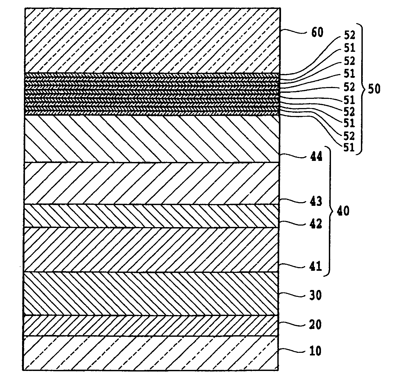
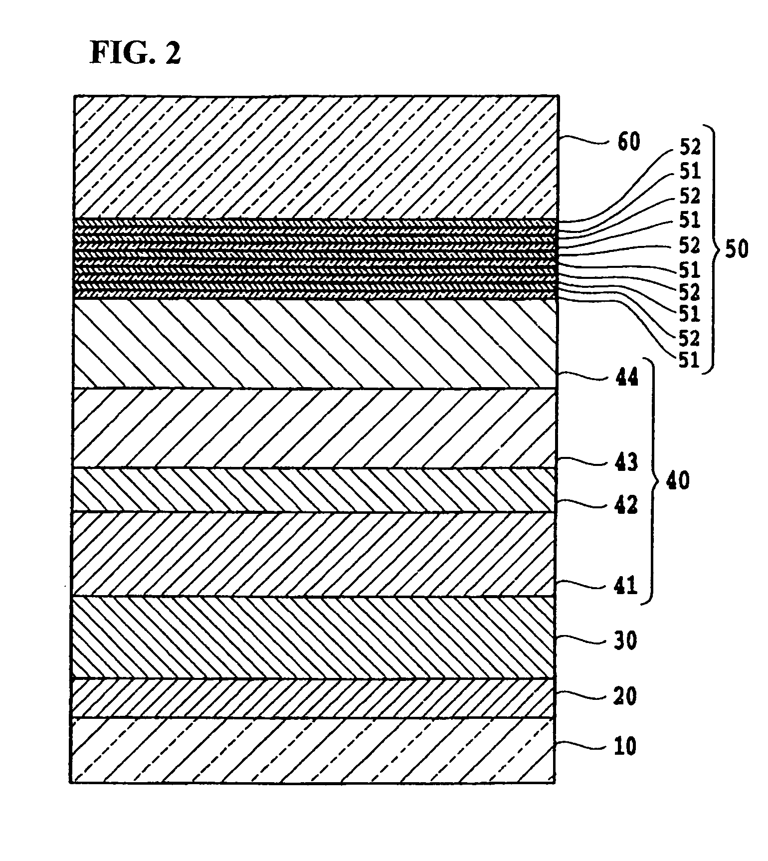
[0068]To evaluate the performance of buffer structures, samples having a multilayer buffer structure on an organic EL layer (electron transport layer) were fabricated. The buffer structure was composed of alternately laminated LiF layers (transparent material layers) and aluminum layers (metallic layers). The samples were fabricated using a three chamber type evaporation apparatus (including a load lock chamber, an organic chamber, and a metal chamber) through the procedure described below. The vacuum chamber was evacuated to 1×10⁻⁵ Pa. The evaporation source used was a resistance heating type. The material of the crucible was quartz, Mo, or BN corresponding to evaporation materials.

[0069]A glass substrate was moved into the organic chamber. An organic EL layer of Alq3 162 nm thick was deposited at a deposition rate of 2 Å / s on the glass substrate. The glass substrate having Alq3 layer thereon was moved to a metal chamber, and a LiF layer 1 nm thick was formed on the Alq3 layer at a...

example 2

[0077]An organic EL device having a buffer structure of a multilayer structure was manufactured as follows.

[0078]A CrB film 100 nm thick was deposited on a glass substrate. After patterning, the processes of drying (at 150° C.) and UV treatment (at room temperature and at 150° C.) were corducted to form a reflective electrode of CrB. Deposition of the CrB film was carried out by a DC sputtering method under room temperature using sputtering gas of argon supplying sputtering power of 300 W.

[0079]The glass substrate with the reflective electrode of CrB formed thereon in the previous steps was moved to an evaporation apparatus. The vacuum chamber was evacuated to 1×10⁻⁵ Pa. Holding the vacuum, an organic EL layer, a buffer structure, and a cathode were sequentially formed. The organic EL layer was comprised of a hole injection layer, a hole transport layer, an organic light emmisive layer, and an electron transport layer. The hole injection layer was formed by depositing copper phthalo...

example 3

[0087]An organic EL device having a multilayered buffer structure was manufactured in the same manner as in Example 2 except that the buffer structure consisting of 10 layers and having total thickness of 10 nm was formed by repeating five times the process of alternately laminating a LiF layer 0.5 nm thick and an aluminum layer 1.5 nm thick. Current density and luminance were measured by applying pulse voltage to the thus obtained organic EL device. The results are given in Table 3.


PUM

PropertyMeasurementUnit
thicknessaaaaaaaaaa
work functionaaaaaaaaaa
thicknessaaaaaaaaaa

Abstract

An organic EL device is disclosed which has a buffer structure that mitigates sputtering damage inflicted in the process of forming a transparent top electrode, that exhibits sufficient electrical conductivity and light transmissivity, and that exhibits high electron injection efficiency. An organic EL device according to the invention includes, sequentially disposed on a substrate, a bottom electrode, an organic EL layer including at least an organic light emissive layer, a buffer structure, and a transparent top electrode through which light is emitted. The buffer structure is a multilayer structure having two or more first type buffer layers containing a transparent material and two or more second type buffer layers containing a metal or an alloy, with each of the second type buffer layers being disposed on one of the first type buffer layers. A method for manufacturing such an organic EL device also is disclosed.

Description

BACKGROUND OF THE INVENTION[0001]The present invention relates to organic light emitting (EL) devices and a method for manufacturing the EL devices, and in particular, to a buffer structure in an organic EL device of a top emission system, and a method for fabricating the structure.[0002]An organic electroluminescence device (hereinafter referred to as an organic EL device) comprising a laminated structure of organic thin films is known as an example of light emission devices applied to display apparatuses. Since C. W. Tang of Eastman Kodak Company disclosed a device with a double layer structure performing high efficient light emission in 1987 (Appl. Phys. Lett. vol. 51, p. 913 (1987)), numerous studies have been made to achieve practical application of organic EL devices.[0003]In recent years there has been extensive development in the field of organic EL displays, particularly in the area of active-matrix drive systems for displays. The display in an active-matrix drive system is...

Claims


Application Information

Patent Timeline
Patent Type & Authority Patents(United States)
IPC IPC(8): H05B33/02B32B19/00H05B33/26H01L51/00H01L51/30H01L51/50H05B33/10
CPCH01L51/5092H01L51/005H01L51/0059H01L51/0078Y10S428/917H01L2251/5315H01L2251/558H01L51/0081H10K85/60H10K85/311H10K85/631H10K85/324H10K50/171H10K2102/3026H10K2102/351H05B33/12H10K50/80
Inventor NAKAMATA, YUKO
Owner FUJI ELECTRIC HLDG CO LTD
Why Eureka
Try Eureka