Methods of manufacturing a lithography template

a technology of lithography and template, applied in the field of lithography templates, can solve the problems of wet etching process suffering from undercutting problems, difficulty in etching opaque materials, pattern defects, etc., and achieves the effects of improving inspectionability, low defect density, and reducing the difficulty of etching

Inactive Publication Date: 2006-05-02
CANON KK
View PDF192 Cites 72 Cited by
  • Summary
  • Abstract
  • Description
  • Claims
  • Application Information

AI Technical Summary

Benefits of technology

[0013]Described herein are methods for making templates for use in lithography systems. The methods described herein are directed to the production of templates with minimal undercut, low defect density, and improved inspectability. These methods are particularly useful for the formation of templates having features that have a lateral feature size of less than about 200 nm. For ultraviolet light curing applications, a template may be formed from an ultraviolet light transmissive substrate. The ultraviolet light transmissive substrate may be formed from a variety of materials (e.g., quartz). Initially, a conductive polysilicon layer is formed on the surface of the substrate. Upon the conductive polysilicon layer, a masking layer is formed. Masking layer may be composed of a photoresist material. The masking la

Problems solved by technology

Etching of the opaque material may be difficult if the opaque material is a metal.
Many metals produce particles and aggregates during a dry etch process which may be deposited on the substrate creating defects in the pattern.
A wet etch process may be used to avoid the deposition of particles, however, wet etching processes suffer from undercutting problems for very small features.
A problem with trying to apply photomask manufacturing process for the manufacture of imprint lithography templates is that the completed photomask tends to have a critical feature size that is generally larger than the feature size that the pattern generation equipment can create.
However, the isotropic etching undercuts the photoresist pattern by about the thickness of the opaque layer or more and makes the openings in the opaque pattern larger than the original openings in photoresist pattern.
For previous generations of semiconductor devices, the undercutting, while not desirab

Method used


Image

  • Methods of manufacturing a lithography template
  • Methods of manufacturing a lithography template
  • Methods of manufacturing a lithography template

Examples


Embodiment Construction

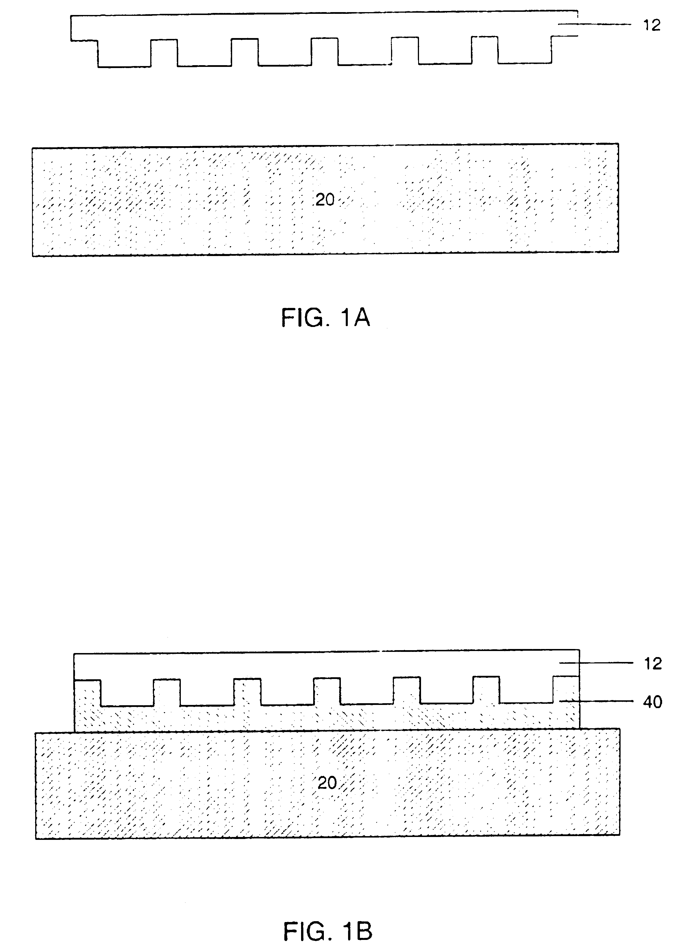
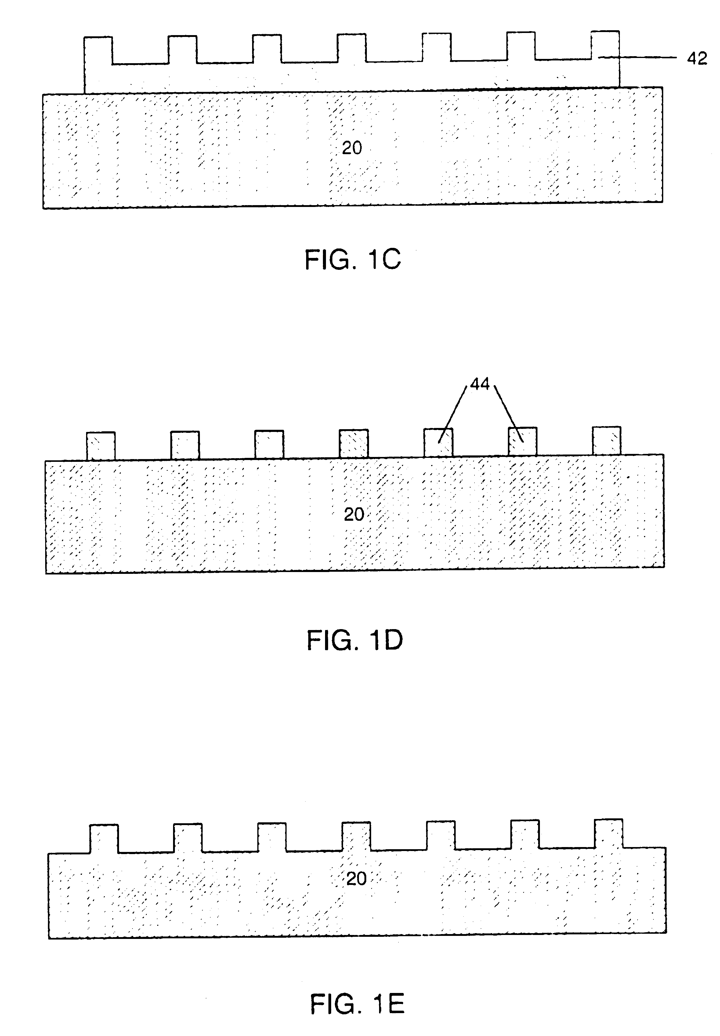
[0025]In general, a method of forming a pattern on a substrate may be accomplished by the use of imprint lithography processes. A typical imprint lithography process includes applying a curable liquid to a substrate, placing a patterned template in contact with the curable liquid, curing the liquid, and removing the template. The pattern of the template is imparted to the cured material disposed on the substrate.

[0026]A typical imprint lithography process is shown in FIGS. 1A through 1E. As depicted in FIG. 1A, template 12 is positioned in a spaced relation to the substrate 20 such that a gap is formed between template 12 and substrate 20. Template 12 may include a surface fabricated to take on the shape of desired features, which in turn, may be transferred to the substrate 20. As used herein, a “feature size” generally refers to a width, length and / or depth of one of the desired features. Surface of template 12 may be treated with a thin layer that lowers the template surface ener...


PUM

PropertyMeasurementUnit
Thicknessaaaaaaaaaa
Electrical conductivityaaaaaaaaaa
Electrical conductoraaaaaaaaaa

Abstract

A method for forming imprint lithography templates is described herein. The method includes forming a masking layer and a conductive layer on a substrate surface. The use of a conductive layer allows patterning of the masking layer using electron beam pattern generators. The substrate is etched using the patterned masking layer to produce a template.

Description

BACKGROUND OF THE INVENTION[0001]1. Field of the Invention[0002]This present invention generally relates to lithography templates. More particularly, certain embodiments of the invention relate to the formation of imprint lithography templates fabricated by pattern generators.[0003]2. Description of the Relevant Art[0004]For imprint lithography, a relief pattern in a template is used, in conjunction with monomers / polymers to imprint a desired pattern into monomers / polymers on the surface of a substrate (e.g., semiconductors, dielectric materials, magnetic or optoelectonic materials.) The processes commonly used to manufacture projection photomasks are often applied to the manufacture of templates for imprint lithography. For this reason, it is useful to provide background of the manufacture of optical projection lithography and optical projection photomasks.[0005]A conventional projection photolithography system projects a UV light pattern onto a light sensitive coating (e.g., a pho...

Claims


Application Information

Patent Timeline
IPC IPC(8): G03F7/00G03F1/00G03F1/34G03F7/09
CPCB82Y10/00B82Y40/00G03F7/093G03F7/0002G03F7/0017G03F1/0084G03F1/34
Inventor VOISIN, RONALD D.
Owner CANON KK
Why Eureka
Try Eureka