Plasma preclean with argon, helium, and hydrogen gases

a technology of argon and hydrogen gas, applied in the direction of vacuum evaporation coating, chemical/physical/physicochemical process, coating, etc., can solve the problems of reducing the electromigration resistance of small features, altering the performance of devices including small features, and sputter etch processes can damage silicon layers by physical bombardment, etc., to achieve the effect of improving etch rate, high aspect ratio, and increasing etch ra

Inactive Publication Date: 2006-05-30
APPLIED MATERIALS INC
View PDF40 Cites 25 Cited by
  • Summary
  • Abstract
  • Description
  • Claims
  • Application Information

AI Technical Summary

Benefits of technology

[0011]The present invention provides a method and apparatus for precleaning a patterned dielectric layer to remove native oxides and polymers of hydrocarbons and fluorinated hydrocarbons from small feature sizes (such as quarter micron widths and smaller) and which may have high aspect ratios. Generally, the present invention provides a method and apparatus for providing a plasma comprising a mixture of argon, helium, and hydrogen to preclean a patterned substrate. Addition of helium to the gas mixture of argon and hydrogen surprisingly increases the etch rate in comparison to argon / hydrogen mixtures. Etch rates are improved for argon concentrations below about 75% by volume. The etch rate actually increases as the argon volume % drops from about 75% to about 25%, and then the etch rate declines as the argon volume % is further reduced.
[0012]Control of the etch rate is provided by controlling the mixture of argon, helium, and hydrogen, and by controlling the chamber pressure. Furthermore, RF power is capacitively and inductively coupled to the plasma to enhance control of the etch properties. Argon, helium, and hydrogen can be provided as separate gases or as mixtures, however, mixing of helium with 5% by volume of hydrogen is preferred for safety and etch performance.

Problems solved by technology

One problem with conventional processes arises because the contact holes or other patterns often comprise high aspect ratios, i.e., the ratio of the height of the holes to their width or diameter is greater than 1.
The presence of native oxides and other contaminants within a small feature typically results in voids by promoting uneven distribution of the depositing metal.
The native oxide and other contaminants create regions on the substrate which interfere with film formation, by creating regions where film growth is stunted.
The presence of native oxides and other contaminants also can increase the via / contact resistance and can reduce the electromigration resistance of small features.
The contaminants can diffuse into the dielectric layer, the sublayer, or the deposited metal and alter the performance of devices which include the small features.
However, sputter etch processes can damage silicon layers by physical bombardment, sputter deposit Si / SiO2 onto sidewalls of the features, and sputter metal sublayers, such as aluminum or copper, onto sidewalls of the features.
For small features having larger aspect ratios, sputter etch processes have not been as effective in removing contaminants within the features, thereby compromising the performance of the devices which are formed.
Preclean by sputter etch processes is particularly unsuitable for features with copper formed or exposed nearby.
Copper easily diffuses through dielectrics, including sidewalls of vias formed in dielectrics, destroying or compromising the integrity of the dielectric.
It is difficult to deposit a uniform metal-containing layer into the high aspect ratio hole 11 because contaminants on the sidewalls 14 of the holes promote uneven deposition of the metal containing layer.
The metal containing layer eventually converge across the width of the hole before it is completely filled, thus forming voids and discontinuities within the metal-containing material.
These voids and discontinuities result in poor and unreliable electrical contacts.

Method used


Image

  • Plasma preclean with argon, helium, and hydrogen gases
  • Plasma preclean with argon, helium, and hydrogen gases
  • Plasma preclean with argon, helium, and hydrogen gases

Examples


example 1

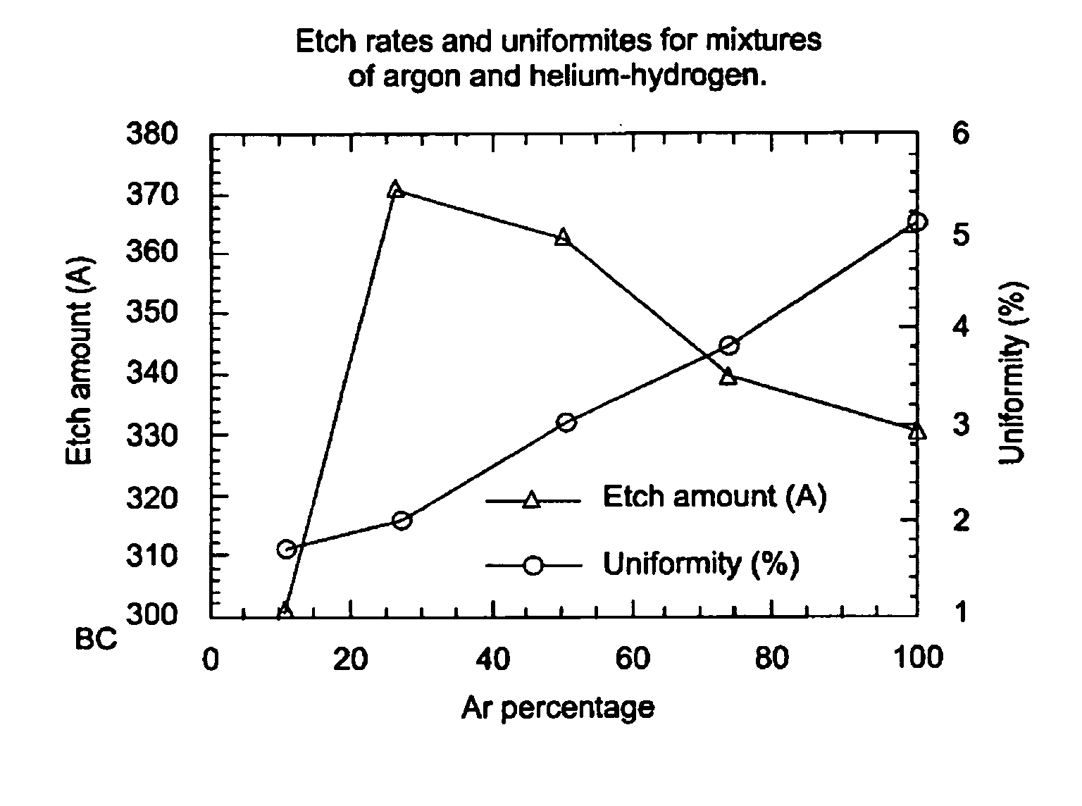
[0033]Examples of the present invention were performed by varying the gas mixture from 100% argon to 10% argon to preclean a patterned substrate surface in a Preclean II chamber on an ENDURA® platform available from Applied Materials, Inc. A silicon wafer having sub 0.30 μm wide contacts, vias, trenches, and other patterns, having an aspect ratio≧4:1 (i.e., a depth of at least 1.20 μm) was introduced into the system. The wafer was then plasma treated with a mixture of argon and He / H2 wherein helium and hydrogen were provided as a mixture having 5% hydrogen by volume.

[0034]Referring to FIG. 4, the etch uniformity drops continuously as the helium mixture is added to the process gas. Further, the etch rate improves until the argon percentage is reduced to 25% by volume.

example 2 (

Comparison)

[0035]For comparison, Example 1 was repeated without the helium. FIG. 5 compares the etch rate for the Ar / He / H2 plasma of Example 1 and the Ar / H2 plasma of Example 2. FIG. 6 compares the etch uniformity for the Ar / He / H2 plasma of Example 1 and the Ar / H2 plasma of Example 2.


PUM

PropertyMeasurementUnit
pressureaaaaaaaaaa
poweraaaaaaaaaa
poweraaaaaaaaaa

Abstract

The present invention provides a method and apparatus for precleaning a patterned substrate with a plasma comprising a mixture of argon, helium, and hydrogen. Addition of helium to the gas mixture of argon and hydrogen surprisingly increases the etch rate in comparison to argon/hydrogen mixtures. Etch rates are improved for argon concentrations below about 75% by volume. RF power is capacitively and inductively coupled to the plasma to enhance control of the etch properties. Argon, helium, and hydrogen can be provided as separate gases or as mixtures.

Description

FIELD OF THE INVENTION[0001]The present invention relates to an apparatus and method for forming integrated plug and wire interconnects on a substrate having submicron features. More particularly, the present invention relates to a sequence for forming metal interconnects wherein a patterned dielectric layer is exposed to a plasma containing an inert gas and a reactive gas.BACKGROUND OF THE INVENTION[0002]Sub-half micron multilevel metallization is one of the key technologies for the next generation of very large scale integration (“VLSI”). The multilevel interconnects that lie at the heart of this technology require planarization of high aspect ratio features such as plugs and other interconnects. Reliable formation of these interconnects is very important to the success of VLSI and to the continued effort to increase circuit density and quality on individual substrates and die.[0003]Conventional chemical vapor deposition (CVD) and physical vapor deposition (PVD) techniques are use...

Claims


Application Information

Patent Timeline
Patent Type & Authority Patents(United States)
IPC IPC(8): H01L21/302B01J19/08C23C14/02C23C16/02H01L21/304H01L21/3065H01L21/311H01L21/768
CPCH01L21/31116H01L21/76877H01L21/76814H01L21/3065
Inventor COHEN, BARNEY M.NGAN, KENNY KING-TAILI, XIANGBING
Owner APPLIED MATERIALS INC
Why Eureka
Try Eureka